What is PCB Manufacturing? A Complete Guide to the Process and Methods
Rachel Roland
In today’s hyper-connected world, nearly every electronic device relies on a hidden hero: the printed circuit board (PCB). From smartphones and laptops to medical devices and automotive systems, PCBs serve as the backbone of modern electronics. But have you ever wondered how these intricate green boards are made? The answer lies in PCB manufacturing—a precise, multi-stage process that transforms design concepts into functional circuitry.
This comprehensive guide dives deep into the world of PCB manufacturing, exploring its core principles, key stages, and various methods used to produce everything from simple prototypes to complex mass-produced boards. Whether you're an engineer, product designer, or simply curious about electronics, understanding this process will give you valuable insight into how your favorite gadgets come to life.
We’ll walk through the entire journey—from initial design and material selection to final testing—and highlight the importance of PCB prototype and PCB sample creation in ensuring quality and performance before full-scale production.
Understanding PCB Manufacturing: The Foundation of Modern Electronics
At its core, PCB manufacturing refers to the process of fabricating printed circuit boards that mechanically support and electrically connect electronic components using conductive pathways, tracks, or signal traces etched from copper sheets laminated onto a non-conductive substrate.
The goal of PCB manufacturing is to create reliable, durable, and efficient platforms for mounting and interconnecting electronic parts like resistors, capacitors, integrated circuits (ICs), and connectors. These boards eliminate the need for bulky wiring harnesses and reduce the risk of loose connections, making them essential in almost all electronic products.
Why PCBs Matter
Before the advent of PCBs, electronic circuits were assembled manually with point-to-point wiring—a time-consuming, error-prone method prone to short circuits and mechanical failure. The introduction of PCBs revolutionized electronics by enabling:
- Miniaturization: Components can be placed closer together.
- Mass production: Boards can be replicated with high consistency.
- Improved reliability: Fewer solder joints and wires mean fewer points of failure.
- Enhanced performance: Controlled impedance and reduced electromagnetic interference (EMI).
Today, PCB manufacturing supports industries ranging from consumer electronics and telecommunications to aerospace, defense, and healthcare.
For companies developing new products, starting with a PCB prototype allows engineers to test functionality, identify design flaws, and optimize layout before committing to large-volume runs. Similarly, producing a PCB sample enables verification of materials, manufacturability, and compliance with specifications.
These early-stage boards are critical for reducing time-to-market and avoiding costly redesigns later in the development cycle.
Key Stages in the PCB Manufacturing Process
Creating a finished PCB involves a series of highly controlled steps, each requiring precision equipment and skilled technicians. While the exact sequence may vary depending on the type of board (e.g., single-sided, double-sided, multilayer), the general flow remains consistent across most PCB manufacturing facilities.
Let’s explore the major phases involved in transforming a digital design into a physical circuit board.
Step 1: Design and Output
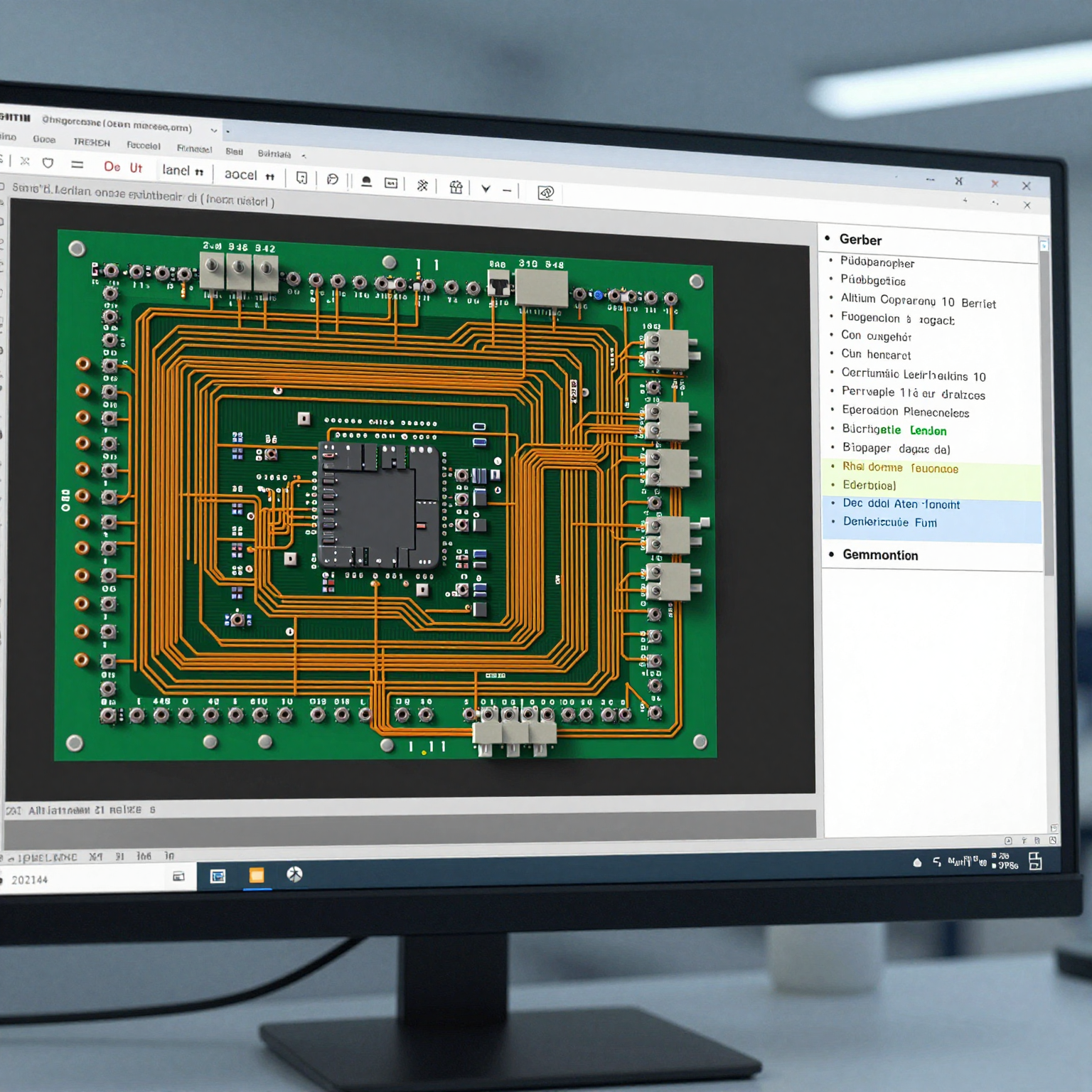
File Preparation
All PCB manufacturing begins with a design created using Electronic Design Automation (EDA) software such as Altium Designer, KiCad, Eagle, or OrCAD. This stage includes:
- Schematic capture
- Component placement
- Routing of electrical connections
- Design rule checking (DRC)
Once finalized, the design is exported into industry-standard file formats used by manufacturers. The most common output files include:
- Gerber Files (.gbr): Define copper layers, solder mask, silkscreen, and drill data.
- NC Drill File: Specifies hole locations and sizes.
- Bill of Materials (BOM): Lists all components needed for assembly.
- IPC-2581 or ODB++: Advanced data formats that bundle all necessary information in one package.
Accuracy at this stage is crucial—any errors in the Gerber files can lead to defective boards. For PCB prototype builds, designers often use simplified versions of their final design to validate core functionality quickly.
Manufacturers typically perform a Design for Manufacturability (DFM) check to ensure the submitted files meet production requirements. This includes verifying trace widths, spacing, via sizes, and layer alignment tolerances.
Pro Tip: Always request a DFM review when ordering a PCB sample, especially if working with tight tolerances or high-density designs.
Step 2: Material Selection and Substrate Preparation
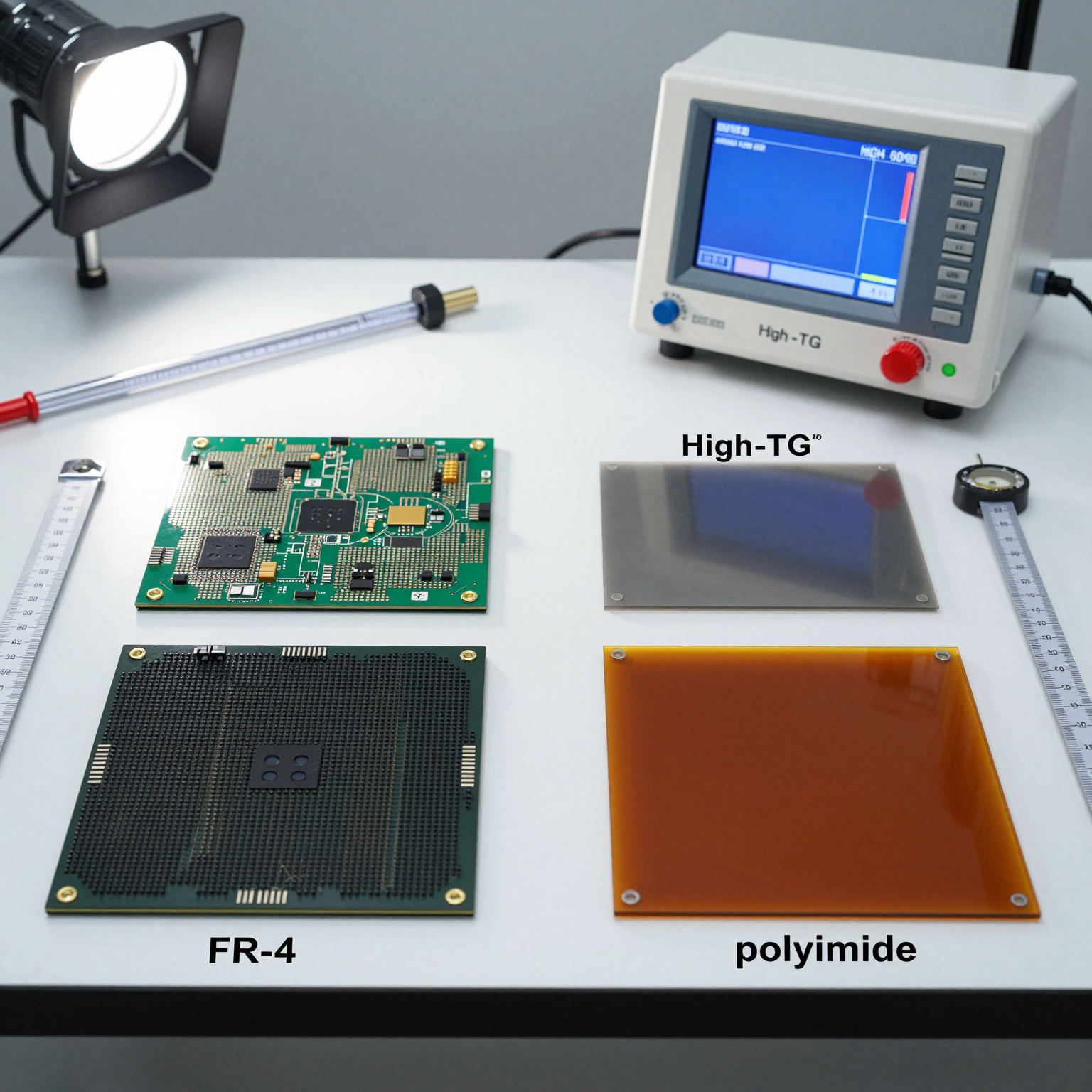
The base material of a PCB—known as the substrate—plays a vital role in determining the board's electrical, thermal, and mechanical properties. Common substrates include:
- FR-4: A glass-reinforced epoxy laminate, widely used due to its excellent insulation, strength, and cost-effectiveness.
- High-Tg FR-4: Offers higher heat resistance, suitable for lead-free soldering processes.
- Polyimide: Used in flexible PCBs (flex PCBs) and high-temperature applications.
- Rogers Material: Preferred for RF and microwave circuits due to low dielectric loss.
- Metal Core (MCPCB): Aluminum-backed boards used in LED lighting and power electronics for better heat dissipation.
Sheets of raw material are cut to size based on panel utilization efficiency. Panels are typically 18” x 24” and contain multiple individual PCBs arranged in arrays to maximize yield during fabrication.
For multilayer boards, additional prepreg (pre-impregnated resin) layers are included between copper foils to bond internal layers together during lamination.
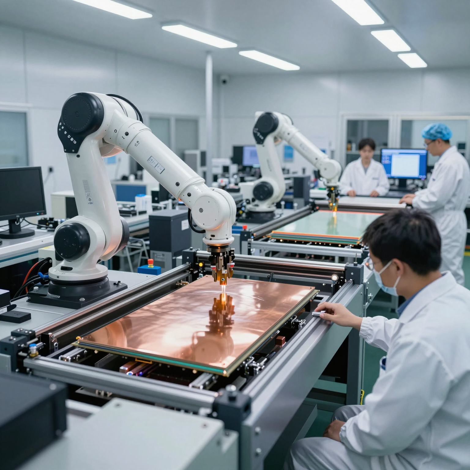
Step 3: Copper Cladding and Layer Alignment
Most PCBs start with a copper-clad laminate—substrate material pre-coated with thin layers of copper foil on one or both sides. In multilayer boards, inner layers are also patterned separately before being stacked.
After cladding, the next step is imaging—the transfer of the circuit pattern onto the copper surface.
Step 4: Imaging and Photolithography
Imaging uses photolithographic techniques similar to those in semiconductor manufacturing. Here’s how it works:
- A photosensitive film called dry film resist is laminated over the copper surface.
- The film is exposed to ultraviolet (UV) light through a photomask containing the circuit pattern.
- Exposed areas become hardened (in positive resists), while unexposed areas remain soluble.
- The board is developed, washing away the unhardened resist and revealing the underlying copper where etching will occur.
Modern facilities use laser direct imaging (LDI) systems instead of physical photomasks, offering higher resolution and eliminating alignment issues associated with traditional masks. LDI is particularly beneficial for HDI (High-Density Interconnect) boards and fine-pitch components.
At this point, only the desired copper traces are protected by the resist; the rest will be removed in the next step.
Step 5: Etching
Etching removes unwanted copper from the board, leaving behind only the conductive pathways defined in the design. The most commonly used etchant is ammonium persulfate or ferric chloride, though some manufacturers use alkaline-based solutions.
The board is sprayed or submerged in the chemical solution, which dissolves exposed copper while preserving the covered traces. After etching, the remaining resist is stripped off, revealing the final copper pattern.
Precision is critical—over-etching can narrow traces beyond specification, affecting conductivity and impedance control. Under-etching leaves excess copper, potentially causing shorts.
For PCB prototype runs, automated optical inspection (AOI) is often performed after etching to detect defects early.
Step 6: Layer Alignment and Lamination (Multilayer Boards Only)
In multilayer PCBs, several etched inner layers must be precisely aligned and bonded together under heat and pressure. Misalignment—even by a fraction of a millimeter—can render the board unusable.
The lamination process involves:
- Stacking inner layers with prepreg sheets acting as adhesive.
- Placing copper foil on top and bottom for outer layers.
- Pressing the stack in a hydraulic press at temperatures up to 375°F (190°C).
- Applying vacuum to remove air bubbles and ensure uniform bonding.
Specialized registration targets (fiducials) on each layer help align them accurately before pressing. Automated X-ray systems verify alignment post-lamination.
Once cooled, the resulting multilayer panel moves to drilling.
Step 7: Drilling Holes
Holes are drilled into the PCB to accommodate component leads (through-hole technology) or to create vias that electrically connect different layers.
Two main types of holes are drilled:
- Through-hole vias: Pass through all layers.
- Blind/buried vias: Connect only specific internal layers (used in HDI PCBs).
Drilling is done using CNC machines equipped with carbide drills as small as 0.1 mm in diameter. High-speed spindles rotate at tens of thousands of RPM to achieve clean cuts without damaging the surrounding material.
Laser drilling is increasingly used for microvias (<0.15 mm), especially in advanced HDI boards. UV lasers offer superior precision and minimal thermal damage compared to mechanical drills.
After drilling, debris is removed via desmearing—a chemical or plasma treatment that cleans resin smear from hole walls, ensuring good adhesion during plating.
Step 8: Electroless and Electroplating
To make vias conductive, the insides of drilled holes must be coated with copper. Since the substrate is non-conductive, a two-step plating process is used:
- Electroless Copper Deposition: A thin layer (~0.5–1 µm) of copper is chemically deposited on the entire surface, including hole walls. This provides a conductive base for electroplating.
- Electroplating: The board is immersed in a copper sulfate bath and subjected to an electric current, which deposits additional copper (typically 20–25 µm thick) on exposed surfaces and within holes.
This step ensures reliable electrical connectivity between layers. Outer layer traces are also reinforced during plating, improving current-carrying capacity.
After plating, excess copper on outer layers is removed through a second round of imaging and etching (subtractive process), leaving only the intended circuit pattern.
Step 9: Solder Mask Application
The solder mask (also known as solder resist) is a protective polymer coating applied to prevent oxidation, corrosion, and accidental short circuits during soldering.
Common colors include green, red, blue, black, and white, with green being the most popular due to its contrast with copper and ease of inspection.
Application methods include:
- Liquid Photoimageable Solder Mask (LPISM): Most common; applied via curtain coating or screen printing, then exposed and developed like photoresist.
- Dry Film Solder Mask: Less common; laminated onto the board.
Openings in the mask expose pads for component mounting and soldering. Vias may also be tented (covered), capped, or left open depending on design needs.
Proper curing is essential—under-cured masks can peel, while over-cured ones become brittle.
Step 10: Silkscreen Printing
Silkscreen (or legend) adds human-readable labels to the board, such as component designators (R1, C2), polarity indicators, logos, and warning symbols.
While traditionally done with inkjet or screen printing, many modern manufacturers use direct legend printing (DLP) for higher accuracy and durability.
Although silkscreen doesn’t affect electrical performance, it plays a vital role in assembly, troubleshooting, and field service.
Note: On high-density boards, silkscreen may be minimized or omitted to avoid interfering with tiny components.
Step 11: Surface Finish Application
The final step in bare PCB fabrication is applying a surface finish to protect exposed copper pads from oxidation and ensure good solderability.
Different finishes offer varying levels of shelf life, flatness, and compatibility with assembly processes. Popular options include:
| Surface Finish | Description | Best For |
|---|---|---|
| HASL (Hot Air Solder Leveling) | Coats pads with molten tin-lead or lead-free alloy, then leveled with hot air | General-purpose, cost-effective |
| Lead-Free HASL | RoHS-compliant version of HASL | Consumer electronics |
| ENIG (Electroless Nickel Immersion Gold) | Nickel barrier layer + thin gold flash | Fine-pitch BGAs, long shelf life |
| ENEPIG | Adds palladium layer; superior wire bonding capability | High-reliability, mixed-signal |
| OSP (Organic Solderability Preservative) | Thin organic coating; environmentally friendly | Short-turn prototypes |
| Immersion Silver/Tin | Metallic coatings with good flatness | High-frequency, flat surfaces |
Choosing the right finish depends on application requirements, component types, and environmental regulations.
For PCB sample evaluation, ENIG or OSP are often preferred due to their flatness and compatibility with SMT assembly.
You can learn more about choosing the best option in our detailed PCB surface finishes guide.
Step 12: Final Testing and Quality Assurance
Before shipment, every batch undergoes rigorous testing to ensure functionality and reliability. Common tests include:
- Automated Optical Inspection (AOI): Detects visual defects like missing traces, shorts, or incorrect markings.
- Electrical Testing (Flying Probe or Bed-of-Nails): Verifies continuity and isolation between nets.
- Microsection Analysis: Cross-sectional examination of vias and plated holes.
- Peel Strength Test: Ensures copper adhesion meets standards.
- Solder Float Test: Evaluates thermal stability during reflow.
For PCB prototype orders, flying probe testing is typically used due to lower setup costs. Mass production runs may use fixture-based bed-of-nails testers for faster throughput.
Quality standards such as IPC-A-600 (acceptability of printed boards) and IPC-6012 (qualification and performance) govern acceptable defect levels.
A well-documented 6-step quality control process helps maintain consistency across production batches.
Types of PCB Manufacturing Methods
Not all PCBs are made the same way. Depending on complexity, volume, and application, manufacturers employ different PCB manufacturing methods tailored to specific needs.
1. Single-Sided PCB Manufacturing
The simplest form of PCB manufacturing, single-sided boards have components and circuitry on only one side of the substrate.
Pros:
- Low cost
- Easy to design and manufacture
- Ideal for basic electronics
Cons:
- Limited routing space
- Not suitable for complex circuits
Applications: Power supplies, LED lighting, sensors, educational kits
Due to their simplicity, PCB prototype versions of single-sided boards can often be produced in just a few days.
2. Double-Sided PCB Manufacturing
Double-sided PCBs feature conductive layers on both the top and bottom, connected via plated-through holes (PTHs).
Pros:
- Higher component density
- Better routing flexibility
- Compact designs possible
Cons:
- More complex than single-sided
- Requires precise alignment
Applications: Industrial controls, amplifiers, instrumentation
This method strikes a balance between cost and functionality, making it ideal for mid-range consumer electronics and PCB sample validation.
3. Multilayer PCB Manufacturing
Multilayer PCBs consist of three or more conductive layers separated by insulating material and bonded together under heat and pressure.
Common configurations include 4-layer, 6-layer, and 8-layer boards, though some advanced designs go up to 30+ layers.
Pros:
- High circuit density
- Improved EMI shielding
- Better power distribution
- Reduced crosstalk
Cons:
- Higher cost
- Longer lead times
- Complex fabrication and testing
Applications: Servers, routers, medical imaging systems, aerospace avionics
Because of their complexity, thorough DFM analysis and careful planning are required before producing a PCB prototype. Many engineers opt for incremental prototyping—starting with simpler versions before scaling up.
4. Rigid PCB Manufacturing
Rigid PCBs are made from solid substrates like FR-4 and maintain a fixed shape throughout their lifecycle.
Pros:
- Mechanically stable
- Easy to mount and assemble
- Wide range of available materials
Cons:
- Cannot bend or flex
- Bulkier than flexible alternatives
Applications: Desktop computers, home appliances, automotive ECUs
Rigid boards dominate the market due to their reliability and compatibility with standard assembly lines.
5. Flexible and Rigid-Flex PCB Manufacturing
Flexible PCBs use polyimide or polyester substrates that allow bending, folding, and dynamic movement.
Rigid-flex boards combine rigid and flexible sections in a single unit, ideal for compact, high-reliability systems.
Pros:
- Space-saving
- Lightweight
- Resistant to vibration and shock
- Enables 3D packaging
Cons:
- Higher cost
- Specialized design and handling required
Applications: Wearables, foldable phones, medical implants, military gear
Designers should follow flexible PCB design best practices to avoid cracking or delamination.
6. HDI (High-Density Interconnect) PCB Manufacturing
HDI technology uses finer lines/spaces, smaller vias (including microvias), and higher connection pad density to pack more functionality into smaller spaces.
Key Features:
- Microvia stacking and staggering
- Blind and buried vias
- Sequential lamination
Pros:
- Enables miniaturization
- Better signal integrity
- Faster signal transmission
Cons:
- Expensive tooling and materials
- Tight process controls required
Applications: Smartphones, tablets, AI accelerators, IoT devices
As demand for smaller, smarter devices grows, HDI is becoming a cornerstone of modern PCB manufacturing. Learn more about the future of this technology in our article on HDI PCB technology.
The Role of PCB Prototypes and Samples in Development
One of the most important aspects of PCB manufacturing is the ability to create PCB prototype and PCB sample units early in the product lifecycle.
What Is a PCB Prototype?
A PCB prototype is an initial version of a circuit board built to test and validate the design before mass production. It allows engineers to:
- Confirm electrical functionality
- Evaluate thermal performance
- Identify layout or routing issues
- Test firmware and software integration
Prototypes are typically produced in small quantities (1–10 units) using rapid turnaround services. Turnkey solutions often include component sourcing and assembly, delivering fully functional boards in days.
Many contract manufacturers offer express PCB manufacturing services specifically designed for prototyping, supporting fast iterations and agile development.
What Is a PCB Sample?
A PCB sample is slightly different—it often refers to a pre-production unit used to verify manufacturability, material compatibility, and process stability. Unlike prototypes focused on function, samples focus on production readiness.
Samples may be used for:
- Customer approval
- Regulatory testing (e.g., FCC, CE)
- Assembly line trials
- Supply chain validation
They help bridge the gap between design and volume production, minimizing risks and delays.
Both PCB prototype and PCB sample stages are integral to reducing development costs and accelerating time-to-market.
Choosing the Right PCB Manufacturer
Selecting a capable PCB manufacturing partner is critical for success. Consider the following factors:
1. Technical Capabilities
Ensure the manufacturer can handle your board’s specifications:
- Layer count
- Minimum trace width/space
- Via types (micro, blind, buried)
- Impedance control
- Special materials (e.g., Rogers, polyimide)
Review their PCB manufacturing capabilities page to confirm compatibility.
2. Quality Standards
Look for certifications like ISO 9001, IPC-A-610, UL, and RoHS compliance. Ask about their PCB quality testing procedures and whether they follow a documented PCB quality control process.
3. Turnaround Time
For urgent projects, choose a supplier offering quick-turn PCB prototype services—some deliver in as little as 24 hours.
4. Support Services
Comprehensive providers offer more than just fabrication. Look for integrated PCB assembly services, electronic component sourcing, and end-to-end supply chain management.
Companies like PCB assembly manufacturer provide turnkey solutions from design to delivery, streamlining the entire process.
5. Communication and Transparency
Clear communication, responsive customer support, and real-time order tracking enhance collaboration. Use the contact PCB manufacturer form to discuss your project details directly.
If you’re ready to move forward, consider submitting a request to get a PCB quote to compare pricing and timelines.
Innovations Shaping the Future of PCB Manufacturing
The PCB manufacturing landscape is evolving rapidly, driven by advances in materials science, automation, and digital engineering.
Smart Factories and Industry 4.0
Modern PCB fabs leverage IoT-enabled machines, AI-driven analytics, and real-time monitoring to improve yield, reduce waste, and enable predictive maintenance.
Digital twins simulate production workflows, allowing virtual testing before physical fabrication.
Additive Manufacturing Techniques
While traditional PCB manufacturing relies on subtractive methods (etching away copper), additive processes are gaining traction. These involve depositing conductive ink only where needed, reducing material waste and enabling novel form factors.
Inkjet and aerosol jet printing allow for conformal electronics on curved surfaces—an exciting frontier for wearables and smart textiles.
Sustainability Initiatives
Environmental concerns are pushing the industry toward greener practices:
- Water recycling in etching and plating
- Lead-free and halogen-free materials
- Energy-efficient equipment
- Waste reduction programs
Regulations like RoHS and REACH continue to shape material choices and disposal protocols.
Advanced Packaging and Embedded Components
Next-generation boards are incorporating embedded passives (resistors, capacitors) and even active ICs within the substrate itself. This reduces footprint, improves performance, and enhances security.
Such innovations require close collaboration between designers and fabricators—highlighting the value of experienced partners.
Conclusion: Mastering PCB Manufacturing for Success
Understanding PCB manufacturing is essential for anyone involved in electronics development. From the initial concept to the final assembled board, each step in the process contributes to the reliability, performance, and scalability of the end product.
Whether you're building a simple PCB prototype to prove a concept or preparing a PCB sample for regulatory approval, knowing the intricacies of fabrication empowers you to make informed decisions.
By leveraging modern PCB manufacturing methods—including multilayer stacking, HDI technology, and advanced surface finishes—you can create innovative, high-performance electronics that meet the demands of today’s market.
And remember: partnering with a trusted provider that offers robust PCB manufacturing services, strong quality assurance, and responsive support can make all the difference in bringing your vision to life.
Ready to start your next project? Explore our full suite of PCB services or visit our PCB blog for more technical insights.