Introduction of Printed Circuit Board Manufacturing: A Comprehensive Guide
Winnie King
In today’s rapidly advancing technological landscape, virtually every electronic device relies on a foundational component: the printed circuit board (PCB). From smartphones and laptops to medical devices and aerospace systems, PCBs serve as the backbone that connects and supports electronic components. The process behind creating these intricate boards—known as printed circuit board manufacturing—is a complex, precision-driven operation involving multiple stages, advanced machinery, and strict quality control protocols.
This comprehensive guide will walk you through the entire journey of printed circuit board producing, covering everything from initial design considerations to final inspection. Whether you're an engineer, product designer, or simply curious about how electronics are made, understanding printed circuit board production offers valuable insight into one of the most critical processes in modern electronics.
What Is a Printed Circuit Board?
A printed circuit board (PCB) is a flat board made from insulating material with conductive pathways etched or printed onto its surface. These pathways connect various electronic components such as resistors, capacitors, integrated circuits (ICs), and connectors. By providing both mechanical support and electrical connectivity, PCBs eliminate the need for bulky wiring harnesses and significantly improve reliability and performance.
PCBs come in various forms:
- Single-sided (one copper layer)
- Double-sided (two copper layers)
- Multilayer (three or more copper layers bonded together)
The complexity of the board depends on the application. Simple consumer gadgets may use single-sided designs, while high-performance computing systems often require multilayer PCBs with dozens of internal layers.
Why Printed Circuit Board Manufacturing Matters
As technology continues to shrink in size while increasing in power, the demand for smaller, faster, and more efficient electronic devices grows exponentially. This places immense pressure on printed circuit board manufacturing to evolve alongside it. Modern PCBs must support higher frequencies, manage heat dissipation, maintain signal integrity, and comply with environmental regulations—all while being cost-effective to produce at scale.
Moreover, industries like telecommunications, automotive, healthcare, defense, and industrial automation depend heavily on reliable PCBs. A failure in the printed circuit board production line can lead to widespread product recalls, safety hazards, or operational downtime. Therefore, mastering the art and science of PCB fabrication is not just important—it's essential.
Overview of the Printed Circuit Board Production Process
The printed circuit board producing process involves several key steps, each requiring specialized equipment, materials, and expertise. Below is a detailed breakdown of the typical workflow used in modern printed circuit board manufacturing facilities.
Step 1: Design and Engineering
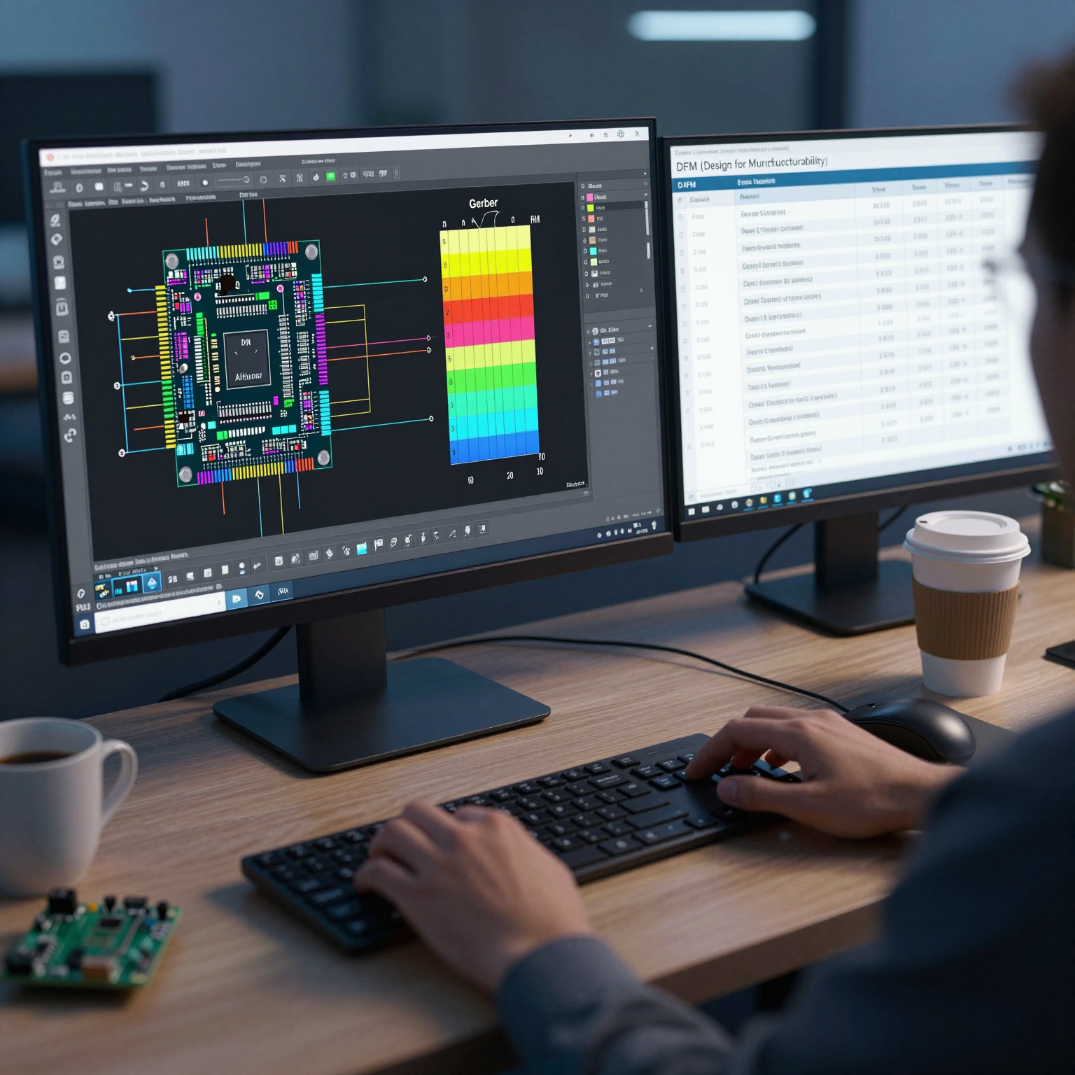
Before any physical production begins, the PCB must be designed using computer-aided design (CAD) software. Engineers create a schematic diagram outlining all components and their interconnections, then translate this into a physical layout known as a Gerber file—the standard format used across the industry.
During this phase, designers consider:
- Component placement
- Trace width and spacing
- Layer stack-up
- Impedance control
- Thermal management
- Electromagnetic compatibility (EMC)
Once finalized, the Gerber files are sent to the manufacturer for review and approval. Many manufacturers offer design-for-manufacturability (DFM) checks to ensure the board can be produced efficiently without errors.
💡 Tip: Always perform a DFM check before finalizing your design. It can save time, reduce costs, and prevent rework later in the printed circuit board production cycle.
Step 2: Material Selection
Choosing the right base material is crucial in printed circuit board manufacturing. The most common substrate is FR-4, a flame-retardant glass-reinforced epoxy laminate. However, other materials like polyimide, PTFE (Teflon), and ceramic-filled hydrocarbons are used for specialized applications such as flexible PCBs or high-frequency RF circuits.
Key properties considered during material selection include:
- Dielectric constant (Dk)
- Dissipation factor (Df)
- Glass transition temperature (Tg)
- Coefficient of thermal expansion (CTE)
- Moisture absorption
For multilayer boards, inner layers are typically made from thin sheets of copper-clad laminate, which are then laminated together under heat and pressure.
Step 3: Printing the Circuit Pattern
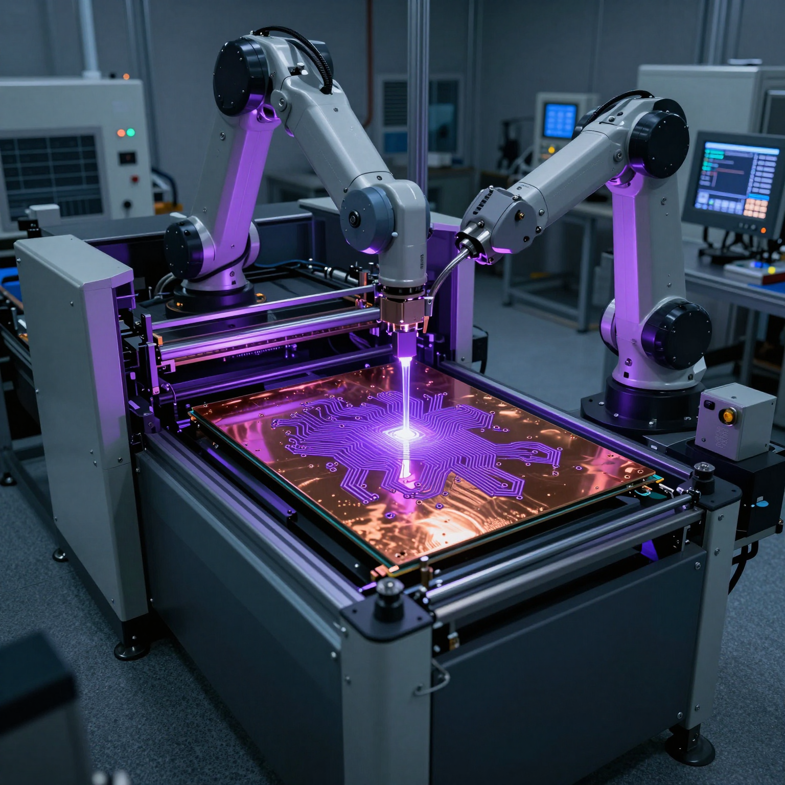
Once materials are selected, the actual printed circuit board producing process begins. The first step is transferring the circuit pattern onto the copper-clad laminate.
Inner Layer Imaging (for Multilayer Boards)
For multilayer PCBs, the inner layers are processed first. A photosensitive film called photoresist is applied to the copper surface. The Gerber data is then used to expose the photoresist through a photomask, defining the circuit pattern.
After exposure, the board undergoes development, where unexposed areas of the photoresist are washed away, leaving only the protected traces. The exposed copper is then etched away using chemical solutions (typically ammonium persulfate or ferric chloride), revealing the desired circuit pattern.
Finally, the remaining photoresist is stripped off, leaving clean copper traces on the inner layer.
Step 4: Etching and Cleaning
Etching is a critical stage in printed circuit board production. It removes unwanted copper while preserving the conductive pathways defined by the imaging process. Precision is vital here—over-etching can narrow traces beyond specification, while under-etching leaves shorts between adjacent lines.
After etching, the panels are thoroughly cleaned to remove residual chemicals and oxidation. They are then inspected for defects using automated optical inspection (AOI) systems.
Step 5: Layer Alignment and Lamination
For multilayer PCBs, individual layers must be precisely aligned and bonded together. This is done using registration holes and alignment pins to ensure perfect stacking.
The stack-up usually consists of:
- Copper layers
- Prepreg (a resin-coated fiberglass sheet acting as an adhesive)
- Core material (pre-made double-sided PCB)
The entire assembly is placed in a hydraulic press and subjected to high temperature and pressure. This melts the prepreg, bonding all layers into a solid, unified structure.
Proper lamination ensures structural integrity and prevents delamination due to thermal cycling or mechanical stress during subsequent processing.
Step 6: Drilling Holes
Holes are drilled into the PCB to allow for component mounting and inter-layer connections. There are two main types:
- Through-hole vias: Pass completely through the board, connecting outer and inner layers.
- Blind and buried vias: Connect only certain layers (used in HDI PCBs).
Modern printed circuit board manufacturing uses CNC drilling machines equipped with carbide drills capable of creating holes as small as 0.1 mm in diameter. For microvias (smaller than 0.15 mm), laser drilling is employed.
Drilling accuracy is paramount—misaligned holes can compromise electrical connections or damage surrounding traces.
Step 7: Plating Through-Holes (PTH)
After drilling, the walls of the holes are plated with copper to establish electrical continuity between layers. This process, known as electroless plating, deposits a thin layer of copper on the non-conductive hole walls.
The board is then subjected to electroplating, which thickens the copper layer to meet specifications. Additional plating may also be applied to the outer surfaces to enhance conductivity and durability.
This step is especially important in ensuring reliable via formation and preventing open circuits in multilayer assemblies.
Step 8: Outer Layer Imaging and Etching
With the internal structure complete, the outer layers undergo a similar imaging and etching process as the inner layers.
Photoresist is applied, exposed using the outer layer Gerber data, developed, and etched. This defines the final circuitry on both top and bottom sides of the board.
Because outer layers often include solder pads and fiducial marks, precision in patterning is even more critical.
Step 9: Solder Mask Application
To protect the copper traces from oxidation and prevent accidental short circuits during assembly, a solder mask is applied. This is typically a polymer coating (often green, but available in red, blue, black, or white) that covers the entire board except for designated areas like pads and vias.
The solder mask is applied via silk screening or liquid photoimageable (LPI) methods, then cured under UV light or heat.
Some advanced processes use selective solder masks to accommodate impedance-controlled traces or fine-pitch components.
You can learn more about different options in our PCB surface finishes guide.
Step 10: Silkscreen Printing
Silkscreen printing adds labels, part numbers, logos, polarity indicators, and other markings to aid in assembly and troubleshooting. While traditionally done with ink, modern methods use inkjet or laser printing for higher precision.
Though not electrically functional, silkscreen information plays a vital role in serviceability and user identification.
Step 11: Surface Finish Application
Since exposed copper oxidizes easily, a protective surface finish is applied to all exposed metal areas (pads, vias, edges). Common finishes include:
- HASL (Hot Air Solder Leveling)
- ENIG (Electroless Nickel Immersion Gold)
- Immersion Silver
- OSP (Organic Solderability Preservative)
- Immersion Tin
Each has advantages depending on shelf life, solderability, wire bonding capability, and cost. For example, ENIG provides excellent flatness for BGA packages, while OSP is environmentally friendly and low-cost.
Selection of the appropriate surface finish is a strategic decision in printed circuit board production, directly affecting downstream assembly yield and long-term reliability.
Step 12: Profiling and Routing
At this stage, individual PCBs are cut out from larger production panels. This is achieved using routing machines or punch presses.
Routing involves using a computer-controlled spindle to mill along predefined paths, separating boards cleanly without damaging edges or components.
V-scoring or tab-routing methods are commonly used when panels contain multiple units, allowing easy depanelization after assembly.
Step 13: Final Inspection and Testing
No printed circuit board manufacturing process is complete without rigorous inspection and testing. Several methods are employed:
Automated Optical Inspection (AOI)
High-resolution cameras scan the board to detect missing traces, shorts, scratches, or misregistrations.
Electrical Testing
Two primary types:
- Flying Probe Test: Uses movable probes to check connectivity and isolation.
- Bed-of-Nails Test: Employs a custom fixture with spring-loaded pins to test all nodes simultaneously.
These tests verify that the board meets the original netlist and functions as intended.
X-ray Inspection (for BGA and Hidden Vias)
Used to inspect internal connections, especially under components like BGAs where visual access is impossible.
Microsectioning (Destructive Testing)
Random samples are cross-sectioned and examined under a microscope to validate plating thickness, layer alignment, and via integrity.
Comprehensive testing ensures compliance with IPC-A-600 and other industry standards.
Step 14: Packaging and Shipping
Once passed, PCBs are cleaned, dried, vacuum-sealed with desiccant packs, and shipped to customers or assembly houses. Proper packaging prevents moisture absorption and electrostatic discharge (ESD) damage.
Many manufacturers follow ESD-safe handling procedures throughout the printed circuit board producing environment to maintain product integrity.
Types of Printed Circuit Boards in Modern Manufacturing
While the core printed circuit board production process remains largely consistent, variations exist based on board type and application requirements.
Rigid PCBs
Most common type; made from solid substrates like FR-4. Used in desktop computers, appliances, and industrial controls.
Flexible PCBs (Flex PCBs)
Made from bendable materials like polyimide. Ideal for compact devices, wearables, and dynamic flexing environments.
Designers should follow flexible PCB design best practices to maximize performance and longevity.
Rigid-Flex PCBs
Combine rigid and flexible sections in a single unit. Often used in military, aerospace, and medical electronics where space and weight are constrained.
High-Density Interconnect (HDI) PCBs
Feature finer lines, tighter spacing, and microvias to achieve higher component density. Essential for smartphones, tablets, and IoT devices.
Learn more about emerging trends in HDI PCB technology.
Metal-Core PCBs (MCPCBs)
Use aluminum or copper bases for superior heat dissipation. Common in LED lighting and power electronics.
RF/Microwave PCBs
Engineered for high-frequency signals with controlled impedance and minimal loss. Require special materials like Rogers or Taconic.
Signal integrity is paramount—see our article on RF PCB design signal integrity for best practices.
Key Challenges in Printed Circuit Board Manufacturing
Despite advances in automation and materials, printed circuit board producing faces several ongoing challenges:
Miniaturization
As devices get smaller, PCBs must accommodate more functionality in less space. This pushes the limits of trace width, via size, and component pitch.
Thermal Management
Increased power density leads to greater heat generation. Poor thermal design can result in premature failure or reduced performance.
Signal Integrity
High-speed digital and RF signals are sensitive to noise, crosstalk, and reflections. Careful routing, grounding, and stack-up planning are required.
Environmental Compliance
Regulations like RoHS (Restriction of Hazardous Substances) and REACH restrict the use of lead, cadmium, and other harmful materials. Manufacturers must adapt processes accordingly.
Supply Chain Volatility
Global disruptions, semiconductor shortages, and raw material price fluctuations impact delivery timelines and costs. Effective PCB supply chain optimization strategies are increasingly important.
Industry Standards and Certifications
To ensure consistency, reliability, and interoperability, the printed circuit board manufacturing industry adheres to several international standards:
- IPC-2221: Generic standard for PCB design
- IPC-6012: Qualification and performance specification for rigid PCBs
- IPC-A-600: Acceptability of printed boards
- ISO 9001: Quality management systems
- UL Certification: Safety certification for electrical equipment
- RoHS/REACH: Environmental compliance
Reputable manufacturers maintain certifications and conduct regular audits to uphold these standards across their printed circuit board production lines.
Innovations Shaping the Future of PCB Manufacturing
The future of printed circuit board producing is being shaped by cutting-edge technologies and evolving market demands.
Additive Manufacturing (3D Printing of PCBs)
Instead of subtractive etching, additive methods deposit conductive ink only where needed. This reduces waste, enables rapid prototyping, and allows for embedded components.
Embedded Components
Passive and active components are being integrated directly within the PCB layers, reducing footprint and improving performance.
Smart Factories and Industry 4.0
IoT-enabled machines, real-time monitoring, predictive maintenance, and AI-driven analytics are transforming traditional printed circuit board manufacturing into smart, responsive operations.
Sustainability Initiatives
Water recycling, lead-free processes, biodegradable substrates, and energy-efficient equipment are becoming standard in eco-conscious factories.
Advanced Materials
New dielectrics with ultra-low Dk/Df values, improved thermal conductivity, and enhanced mechanical strength are enabling next-generation 5G, AI, and autonomous systems.
Choosing the Right PCB Manufacturer
Selecting a capable printed circuit board manufacturing partner is crucial for product success. Consider the following factors:
Technical Capabilities
Can they handle your required layer count, via types, impedance control, and surface finishes? Review their PCB manufacturing capabilities to ensure alignment with your project needs.
Quality Assurance
Look for robust QA systems, including AOI, flying probe testing, X-ray inspection, and adherence to IPC standards. A transparent 6-step quality control process indicates commitment to excellence.
Turnaround Time
Prototypes and time-to-market are critical. Evaluate whether the manufacturer offers quick-turn services without sacrificing quality.
Customer Support
Responsive communication, engineering support, and DFM feedback streamline collaboration.
Cost vs. Value
While cost matters, prioritize value—reliability, yield, and long-term partnership potential often outweigh minor price differences.
If you're looking for a trusted partner, consider reaching out to a professional PCB assembly manufacturer who offers end-to-end solutions from fabrication to full turnkey assembly.
Integration with PCB Assembly Services
It's important to note that printed circuit board manufacturing is only the first half of the story. Once bare boards are produced, they must be populated with components—a process known as PCB assembly.
There are two primary methods:
- Surface Mount Technology (SMT): Components are mounted directly onto the surface.
- Through-Hole Technology (THT): Leads are inserted into drilled holes and soldered on the opposite side.
Many modern products use a combination of both. Understanding the differences between SMT vs through-hole assembly helps optimize design choices.
Full-service providers offer seamless integration between printed circuit board production and assembly, reducing logistics complexity and improving traceability.
Additional services such as electronic component sourcing, programming, conformal coating, and box build further simplify the supply chain.
Conclusion: The Backbone of Modern Electronics
Printed circuit board manufacturing is a sophisticated, multi-stage discipline that lies at the heart of modern electronics. From the initial concept to the final tested board, every step requires precision, expertise, and attention to detail.
As technology evolves, so too does the printed circuit board producing industry—pushing boundaries in miniaturization, performance, and sustainability. Whether you're developing a simple prototype or launching a complex commercial product, understanding the fundamentals of printed circuit board production empowers better design decisions, smoother manufacturing, and higher-quality outcomes.
By partnering with experienced manufacturers, leveraging industry best practices, and staying informed about innovations, businesses can navigate the complexities of PCB fabrication with confidence.
Ready to bring your next project to life? Explore our range of PCB services, or contact PCB manufacturer today to discuss your requirements and get a quote.