PCB Manufacturing Assembly: From Prototypes to HDI and Rigid-Flex Solutions
Rossannie Rolling
The Evolution and Importance of Modern PCB Manufacturing Assembly
In today's hyper-connected technological landscape, the demand for smarter, faster, and more compact electronic devices has never been greater. At the heart of every modern electronic device—ranging from smartphones and wearables to medical equipment and aerospace systems—lies a critical component: the printed circuit board (PCB). As technology evolves, so too does the complexity and sophistication required in PCB Manufacturing Assembly processes.
Modern electronics are no longer limited to simple single-layer boards with through-hole components. Instead, they require advanced solutions such as flexible PCBs (FPC), high-density interconnect (HDI) designs, and rigid-flex hybrids that combine durability with spatial adaptability. These innovations have redefined what is possible in product design, enabling miniaturization, improved performance, and enhanced reliability across industries.
This article delves into the intricate world of PCB Manufacturing Assembly, exploring key technologies like FPC Manufacturing Assembly, PCB prototype Assembly, HDI Manufacturing Assembly, and Rigid-flex Manufacturing Assembly. We will examine their unique characteristics, manufacturing challenges, applications, and how partnering with an experienced PCB assembly manufacturer can ensure success in bringing complex electronic products to market.
Why PCB Manufacturing Assembly Matters
The term PCB Manufacturing Assembly refers not only to the fabrication of bare circuit boards but also to the complete process of populating them with electronic components to create functional units known as PCBA (Printed Circuit Board Assembly). This dual-phase process includes:
- PCB Fabrication: Creating the physical board using copper layers, substrates, solder masks, and silkscreens.
- Component Assembly: Mounting and soldering electronic parts via surface mount technology (SMT), through-hole technology (THT), or mixed-mode processes.
Each stage demands precision engineering, strict adherence to design specifications, and rigorous quality control. A failure at any point can lead to costly delays, field failures, or safety risks—especially in mission-critical sectors like healthcare, automotive, and defense.
As consumer expectations rise and product lifecycles shorten, manufacturers must adopt agile, scalable, and technologically advanced PCB Manufacturing Assembly strategies. Whether producing low-volume prototypes or high-volume production runs, the ability to deliver consistent quality while meeting tight deadlines is paramount.
Understanding Key Types of PCB Manufacturing Assembly
While traditional rigid PCBs remain widely used, advancements in materials science and manufacturing techniques have led to specialized forms of PCB Manufacturing Assembly tailored for specific performance needs. Below, we explore four major categories driving innovation in electronics today.
FPC Manufacturing Assembly: Flexibility Meets Functionality
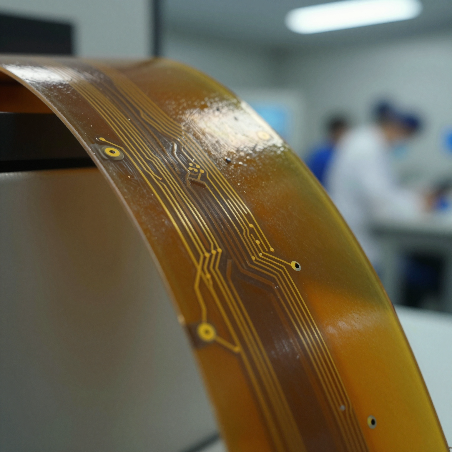
Flexible Printed Circuits (FPCs) represent a revolutionary shift from rigid boards by offering bendable, lightweight alternatives ideal for space-constrained or dynamic environments. FPC Manufacturing Assembly involves creating circuits on flexible polymer substrates such as polyimide or polyester, allowing the board to conform to 3D shapes or withstand repeated flexing.
Advantages of FPCs:
- Space Efficiency: Enables compact designs in wearable tech, foldable displays, and IoT sensors.
- Weight Reduction: Ideal for aerospace and portable medical devices where every gram counts.
- Improved Reliability: Fewer connectors and interconnects reduce potential points of failure.
- Dynamic Flexing Capability: Suitable for moving parts like printer heads or robotic joints.
However, FPC Manufacturing Assembly presents unique challenges:
- Handling delicate materials during SMT requires specialized tooling and fixtures.
- Thermal expansion differences between components and flexible substrates can cause warping.
- Impedance control and signal integrity become more complex due to variable trace geometry.
Applications include smartphone cameras, hearing aids, automotive infotainment systems, and implantable medical devices. For engineers designing next-generation electronics, understanding FPC Manufacturing Assembly best practices is essential. Resources like the flexible PCB design best practices guide offer valuable insights into layout considerations, material selection, and manufacturability.
Fun Fact: Apple’s iPhone uses multiple FPCs to connect the display, camera, and buttons—allowing for slim profiles and seamless integration.
PCB Prototype Assembly: Accelerating Product Development
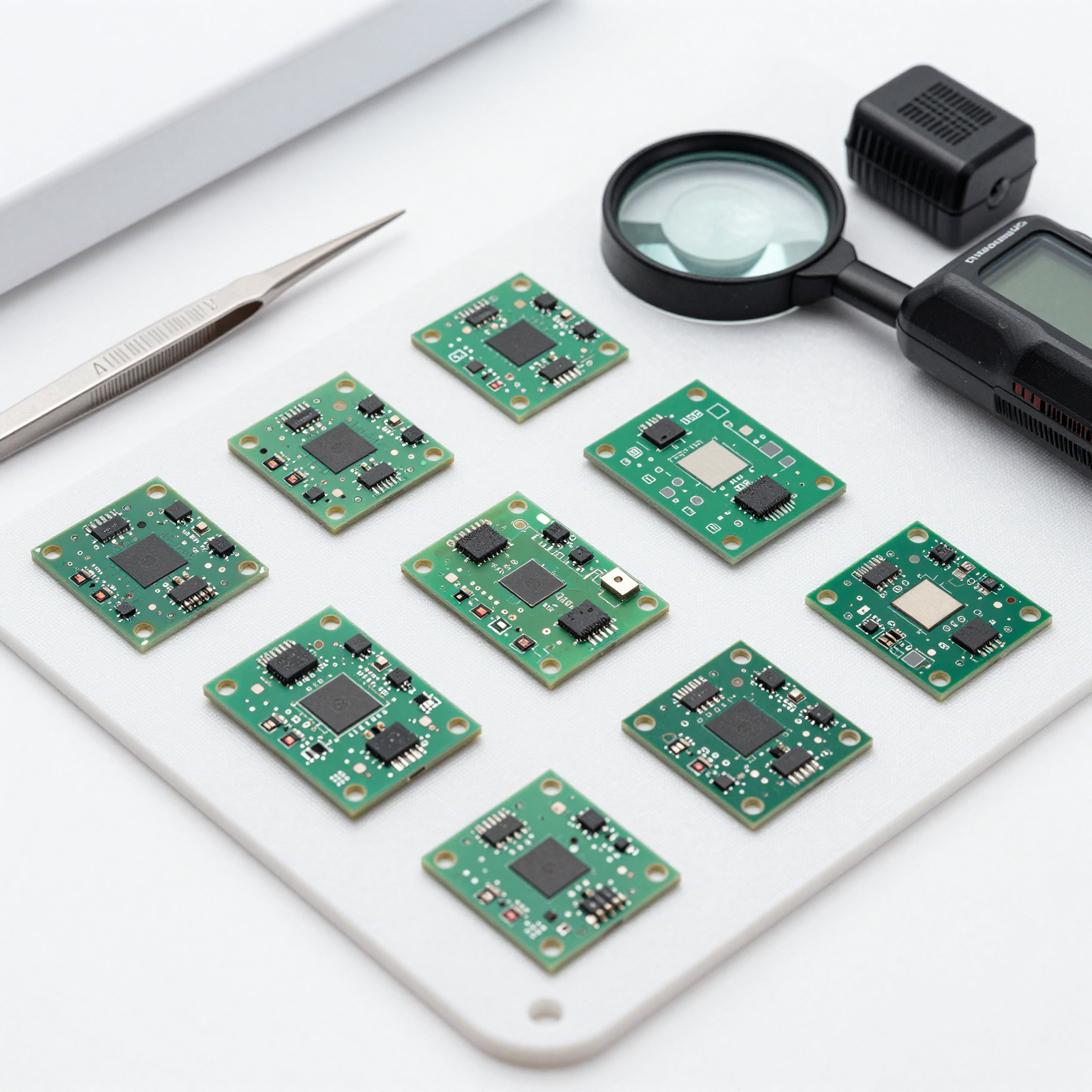
Before mass production begins, validating a design through PCB prototype Assembly is crucial. This phase allows engineers to test functionality, identify design flaws, and refine performance under real-world conditions.
Benefits of Early Prototyping:
- Reduces time-to-market by catching issues early.
- Lowers development costs by avoiding large-scale rework.
- Facilitates compliance testing (EMC, thermal, mechanical).
- Supports investor demonstrations and pre-launch marketing.
Modern PCB prototype Assembly services leverage rapid-turn manufacturing capabilities, often delivering fully assembled boards within 24–72 hours. These fast-turn services use automated optical inspection (AOI), X-ray inspection for BGA packages, and flying probe testing to ensure quality even at small volumes.
Key considerations when ordering prototypes:
- Use standardized component footprints compatible with automated assembly.
- Provide clear Gerber files, BOMs (Bill of Materials), and assembly drawings.
- Specify preferred surface finishes (e.g., ENIG, HASL, Immersion Silver).
For startups and R&D teams, access to reliable PCB prototype Assembly partners streamlines innovation. The prototype PCB assembly guide offers step-by-step instructions on preparing files and selecting appropriate manufacturing options.
Moreover, many full-service providers offer turnkey prototyping, handling everything from bare board fabrication to component sourcing and final testing—eliminating supply chain complexities for clients.
HDI Manufacturing Assembly: Powering High-Density Electronics
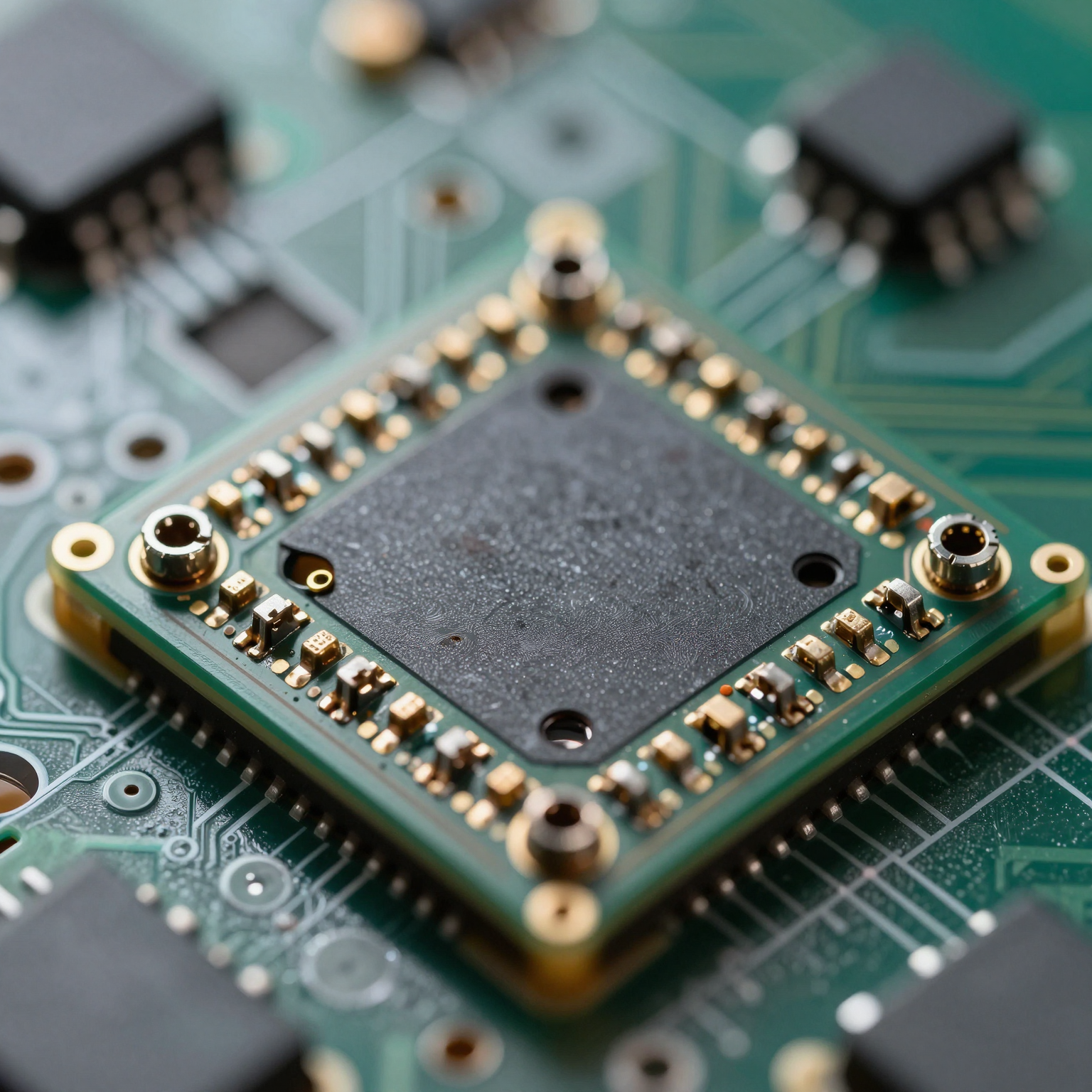
High-Density Interconnect (HDI) technology enables significantly higher component density and faster signal transmission compared to conventional PCBs. HDI Manufacturing Assembly utilizes microvias (typically <150µm), blind/buried vias, and finer line widths to pack more functionality into smaller spaces.
Core Features of HDI Boards:
- Microvia drilling using laser ablation.
- Sequential lamination processes.
- Higher layer count with reduced thickness.
- Enhanced electrical performance and reduced EMI.
These features make HDI boards ideal for:
- Smartphones and tablets
- AI accelerators and GPUs
- Advanced driver-assistance systems (ADAS)
- Miniaturized medical implants
Despite their advantages, HDI Manufacturing Assembly demands exceptional precision:
- Misalignment in microvia stacking can lead to open circuits or shorts.
- Resin smearing during drilling affects plating quality.
- Tight tolerances require advanced imaging and registration systems.
Quality assurance becomes even more critical, with AOI, cross-sectional analysis, and impedance testing forming part of standard validation protocols. Innovations such as stacked and staggered microvias continue to push the boundaries of miniaturization.
Industry trends suggest growing adoption of HDI Manufacturing Assembly in 5G infrastructure, edge computing, and augmented reality headsets. According to recent research published by IEEE Xplore, HDI-based modules show up to 40% improvement in signal propagation speed over traditional multilayer boards.
For deeper insight into emerging trends, read the HDI PCB technology trends blog post covering future developments in substrate materials and via formation techniques.
Rigid-Flex Manufacturing Assembly: Combining Strength and Adaptability
Combining the structural stability of rigid boards with the flexibility of FPCs, Rigid-flex Manufacturing Assembly delivers hybrid solutions optimized for harsh environments and complex packaging requirements.
A typical rigid-flex board consists of:
- Multiple rigid sections made from FR-4 or similar laminates.
- Flexible layers (polyimide) acting as internal hinges or external connections.
- ZIF (Zero Insertion Force) contacts or direct bonding interfaces.
Key Applications:
- Military and aerospace avionics
- Downhole oil & gas sensors
- Surgical robotics
- Foldable consumer electronics
Advantages include:
- Elimination of cables and connectors, reducing weight and failure points.
- Improved shock and vibration resistance.
- 3D packaging capability for compact enclosures.
Challenges in Rigid-flex Manufacturing Assembly:
- Complex stack-up planning requiring precise alignment between rigid and flex zones.
- Differential thermal expansion affecting solder joint integrity.
- Specialized testing jigs due to non-planar geometries.
Successful implementation depends heavily on collaboration between designers and manufacturers early in the development cycle. Design for manufacturability (DFM) reviews help prevent issues related to bending radii, coverlay placement, and stiffener integration.
Manufacturers equipped with advanced lamination presses, laser drill systems, and 3D metrology tools are better positioned to deliver high-reliability Rigid-flex Manufacturing Assembly outcomes. Companies serving defense and aerospace sectors often adhere to IPC-6013 Class 3 standards for flexible and rigid-flex boards.
The Integrated Workflow of PCB Manufacturing Assembly
To fully appreciate the scope of PCB Manufacturing Assembly, it’s important to understand the end-to-end workflow—from initial design to final product delivery. While each type (FPC, HDI, rigid-flex) has unique steps, the general flow remains consistent across most advanced assemblies.
Step 1: Design and File Preparation
Engineers begin with schematic capture and PCB layout using EDA tools like Altium Designer, KiCad, or Cadence Allegro. Critical outputs include:
- Gerber files (RS-274X format)
- NC drill files
- Bill of Materials (BOM)
- Pick-and-place file
- Assembly and fabrication drawings
Design rules must align with the chosen PCB Manufacturing Assembly method:
- Minimum trace/space for HDI
- Bend radius guidelines for FPC
- Via aspect ratios for rigid-flex
Using impedance calculators and DFM checkers ensures compatibility with manufacturing capabilities.
Step 2: Material Selection and Stack-Up Planning
Choosing the right base materials is foundational. Common choices include:
- FR-4: Standard epoxy-glass laminate for rigid boards
- Polyimide: High-temperature resistant film for FPCs
- Rogers: RF-optimized dielectrics for high-frequency apps
- BT Epoxy: Used in HDI substrates for thermal stability
Stack-up configuration defines layer order, dielectric thickness, and impedance targets. For HDI Manufacturing Assembly, sequential build-up (SBU) methods may be employed to add layers incrementally.
Step 3: Bare Board Fabrication
Fabrication transforms raw materials into finished bare PCBs. Processes vary slightly depending on board type but generally involve:
For All Boards:
- Inner layer imaging and etching
- Lamination (for multilayer)
- Drilling (mechanical/laser)
- Plating (PTHs and surface finishes)
Specialized Steps:
- FPC: Coverlay application, stiffener bonding
- HDI: Laser drilling of microvias, sequential lamination
- Rigid-flex: Selective lamination, controlled-depth routing
After fabrication, boards undergo electrical testing (flying probe or bed-of-nails) and visual inspection.
Step 4: Component Sourcing and Procurement
Once bare boards are ready, the next phase in PCB Manufacturing Assembly is acquiring electronic components. This can be managed in-house or outsourced to a contract manufacturer offering electronic component sourcing services.
Challenges include:
- Long lead times for obsolete or in-demand parts (e.g., MCUs during chip shortages)
- Risk of counterfeit components
- Obsolescence management
Reputable manufacturers maintain relationships with authorized distributors and employ screening methods like X-ray analysis and decapsulation testing to verify authenticity.
For guidance on navigating procurement hurdles, refer to the electronic components sourcing guide, which outlines best practices for inventory planning and risk mitigation.
Step 5: Surface Mount and Through-Hole Assembly
Assembly marks the transition from passive board to active electronic system. Two primary methods dominate:
Surface Mount Technology (SMT):
- Components placed directly onto pads using pick-and-place machines.
- Reflow soldering melts solder paste to form electrical and mechanical bonds.
- Ideal for small, high-pin-count devices (QFPs, BGAs, 0201 passives).
SMT lines typically include:
- Solder paste printer
- SPI (Solder Paste Inspection)
- Pick-and-place machine
- Reflow oven
- AOI station
Through-Hole Technology (THT):
- Leads inserted into plated holes and soldered on the opposite side.
- Wave soldering or selective soldering used for批量processing.
- Still relevant for power components, connectors, and ruggedized designs.
Many modern PCB Manufacturing Assembly operations use hybrid lines combining both SMT and THT for maximum versatility.
Special attention is needed for challenging components like Ball Grid Arrays (BGAs), which require X-ray inspection to validate hidden solder joints. The BGA assembly challenges article explores common defects and mitigation strategies.
Step 6: Final Testing and Quality Assurance
No PCB Manufacturing Assembly process is complete without thorough testing. Depending on application requirements, tests may include:
- Automated Optical Inspection (AOI): Detects missing, misaligned, or damaged components.
- X-ray Inspection (AXI): Validates internal connections (BGAs, QFNs).
- In-Circuit Testing (ICT): Checks individual component values and shorts/opens.
- Functional Testing (FCT): Simulates real-world operation.
- Environmental Stress Screening (ESS): Thermal cycling, vibration testing.
A robust QA strategy follows structured methodologies like the 6-step quality control process, ensuring traceability, corrective actions, and continuous improvement.
Certifications such as ISO 9001, IATF 16949 (automotive), and AS9100 (aerospace) further validate a manufacturer’s commitment to excellence.
Industry Applications Driving Demand for Advanced PCB Manufacturing Assembly
The rise of smart, connected, and autonomous systems has fueled demand for sophisticated PCB Manufacturing Assembly solutions across diverse sectors.
Consumer Electronics
Smartphones, tablets, wearables, and smart home devices rely heavily on HDI Manufacturing Assembly and FPC Manufacturing Assembly to achieve sleek form factors and high performance. Foldable phones, for instance, depend on ultra-thin, durable rigid-flex Manufacturing Assembly to enable screen articulation without breaking circuits.
Market data from Statista indicates that global smartphone shipments exceeded 1.4 billion units in 2024, underscoring the scale of demand for advanced PCBs.
Medical Devices
Implantable pacemakers, hearing aids, endoscopic cameras, and portable diagnostics benefit from miniaturized PCB prototype Assembly and HDI Manufacturing Assembly. Biocompatible coatings, hermetic sealing, and ultra-reliable interconnects are standard requirements.
Regulatory compliance (FDA, CE Mark) necessitates stringent documentation and validation throughout the PCB Manufacturing Assembly lifecycle.
Automotive and EVs
Modern vehicles contain over 100 electronic control units (ECUs), managing everything from engine performance to infotainment and ADAS. Electric vehicles (EVs) intensify this trend with battery management systems (BMS), motor controllers, and charging modules—all demanding high-power, thermally efficient PCB Manufacturing Assembly.
Autonomous driving systems require HDI-based radar and lidar processing units capable of handling terabytes of sensor data per hour.
Industrial Automation and IoT
Robots, programmable logic controllers (PLCs), and wireless sensors deployed in factories use ruggedized rigid-flex Manufacturing Assembly to endure vibration, temperature extremes, and electromagnetic interference.
Edge computing nodes increasingly integrate AI chips on HDI substrates, enabling real-time decision-making without cloud dependency.
Aerospace and Defense
Military radars, satellite communication systems, and UAVs operate in extreme conditions requiring radiation-hardened, high-reliability PCB Manufacturing Assembly. Rigid-flex boards eliminate connectors prone to failure in high-G environments.
Standards like MIL-PRF-31032 and IPC-6012/6013 govern performance and qualification testing.
Choosing the Right Partner for Your PCB Manufacturing Assembly Needs
Selecting a capable PCB assembly manufacturer is one of the most strategic decisions in product development. Factors to consider include:
Technical Capabilities
- Can they handle your required technologies (HDI, FPC, rigid-flex)?
- Do they support fine-pitch components, microvias, and impedance control?
- What surface finishes do they offer (ENIG, OSP, Immersion Tin)?
Visit the PCB manufacturing capabilities page to assess a vendor’s equipment, certifications, and process maturity.
Supply Chain Resilience
- Do they have strong component sourcing networks?
- Can they manage obsolescence and mitigate shortage risks?
- Are they transparent about alternative parts?
Look for partners offering full turnkey services, reducing coordination overhead.
Quality Systems
- Are they certified to ISO, IPC, or industry-specific standards?
- What testing and inspection methods do they employ?
- Is there traceability down to lot level?
A documented 6-step quality control process demonstrates systematic rigor.
Scalability and Turnaround
- Can they support NPI (New Product Introduction), pilot runs, and volume scaling?
- What are their typical lead times for prototypes vs. production?
- Do they offer DFM feedback before committing to build?
Fast-turn PCB prototype Assembly services accelerate learning cycles.
Customer Support and Communication
- Is there a dedicated project manager?
- How responsive are they to queries and change requests?
- Do they provide real-time order tracking?
Strong communication prevents misunderstandings and keeps projects on schedule.
For organizations seeking comprehensive solutions, evaluating a company’s industries served by PCB manufacturer helps determine domain expertise.
Ultimately, successful partnerships are built on trust, transparency, and shared goals. Requesting samples, visiting facilities (or virtual tours), and reviewing customer testimonials can provide confidence in a manufacturer’s abilities.
Future Trends Shaping PCB Manufacturing Assembly
As Moore’s Law slows and new paradigms emerge, PCB Manufacturing Assembly continues to evolve. Emerging trends include:
Embedded Components
Passive and active components embedded within PCB layers reduce footprint and improve signal integrity—pushing the envelope of HDI Manufacturing Assembly.
Additive Manufacturing
3D printing of conductive traces enables rapid prototyping of complex interconnects without traditional etching processes.
Sustainability Initiatives
Lead-free processes, recyclable substrates, and energy-efficient manufacturing aim to reduce environmental impact.
AI-Driven Optimization
Machine learning algorithms optimize solder paste deposition, predict defect rates, and enhance yield management in PCB Manufacturing Assembly lines.
According to a report by McKinsey & Company, heterogeneous integration and advanced packaging will drive tighter convergence between ICs and PCBs, blurring traditional boundaries.
These innovations promise to unlock new possibilities in wearable health monitors, quantum computing modules, and brain-machine interfaces.
Conclusion: Mastering the Complexity of PCB Manufacturing Assembly
From FPC Manufacturing Assembly enabling foldable displays to HDI Manufacturing Assembly powering AI chips, the evolution of PCB Manufacturing Assembly reflects broader technological progress. Each advancement—whether in materials, processes, or integration—brings new opportunities and challenges.
Understanding the nuances of PCB prototype Assembly, rigid-flex Manufacturing Assembly, and other specialized techniques empowers engineers and product managers to make informed decisions. By leveraging expert partners with proven capabilities in these domains, businesses can accelerate innovation, reduce risk, and deliver superior products to market.
Whether you're developing a cutting-edge medical device or scaling up consumer electronics, investing in the right PCB Manufacturing Assembly strategy is essential. Explore available resources, engage with qualified suppliers, and take advantage of turnkey services to streamline your journey from concept to commercialization.
To learn more about advanced assembly methods, visit our detailed guide on the complete guide to PCB assembly. And if you’re ready to move forward, don’t hesitate to contact PCB manufacturer for a consultation or get a PCB quote tailored to your project’s needs.