RF PCB Design: Managing Signal Integrity at High Frequencies
John Doe
In today’s fast-evolving electronics landscape, Radio Frequency (RF) printed circuit boards (PCBs) are at the heart of countless wireless technologies — from 5G infrastructure and satellite communications to IoT devices and radar systems. As operating frequencies climb into the GHz range, managing signal integrity becomes one of the most critical challenges in RF PCB design.
For engineers and product developers, ensuring clean, reliable signal transmission at high frequencies PCB is no longer optional — it's essential. Poor signal integrity can lead to data corruption, reduced performance, electromagnetic interference (EMI), and even complete system failure.
At SUNTOP Electronics, a trusted PCB assembly manufacturer, we understand the intricacies of RF design. We specialize in producing high-performance RF PCBs that meet stringent electrical and mechanical requirements, from initial concept to High Frequencies PCB Prototype and full-scale production.
Why Signal Integrity Matters in RF PCB Design
Signal integrity refers to the ability of an electrical signal to propagate through a circuit without distortion. In low-frequency designs, this is often taken for granted. However, as frequencies increase, parasitic effects such as capacitance, inductance, and impedance mismatches become dominant factors.
In RF PCB design, signals behave more like waves than simple currents. At microwave frequencies (typically above 1 GHz), wavelengths become comparable to trace lengths on the board. This means even small discontinuities — such as vias, bends, or layer transitions — can cause reflections, crosstalk, and attenuation.
Key consequences of poor signal integrity include:
- Signal reflection due to impedance mismatch
- Crosstalk between adjacent traces
- Attenuation leading to weak signal strength
- Phase noise and jitter affecting timing
- Electromagnetic interference (EMI) disrupting nearby circuits
These issues are not only difficult to debug post-manufacture but can also significantly delay time-to-market if not addressed during the design phase.
Core Challenges in High Frequencies PCB Design
Designing for high-frequency operation introduces several unique challenges that demand careful planning and precision engineering.
1. Impedance Control
Maintaining controlled impedance is fundamental in RF PCB design. Most RF systems operate with standard impedances like 50Ω or 75Ω. Any deviation along the signal path — whether from trace width variation, dielectric thickness changes, or material inconsistency — causes reflections.
To ensure consistent impedance:
- Use precise stack-up planning
- Calculate trace dimensions using field solvers
- Specify tight tolerances for fabrication (e.g., ±0.1 mm trace width)
Advanced tools like Ansys HFSS or Keysight ADS help simulate impedance behavior before prototyping.
2. Dielectric Material Selection
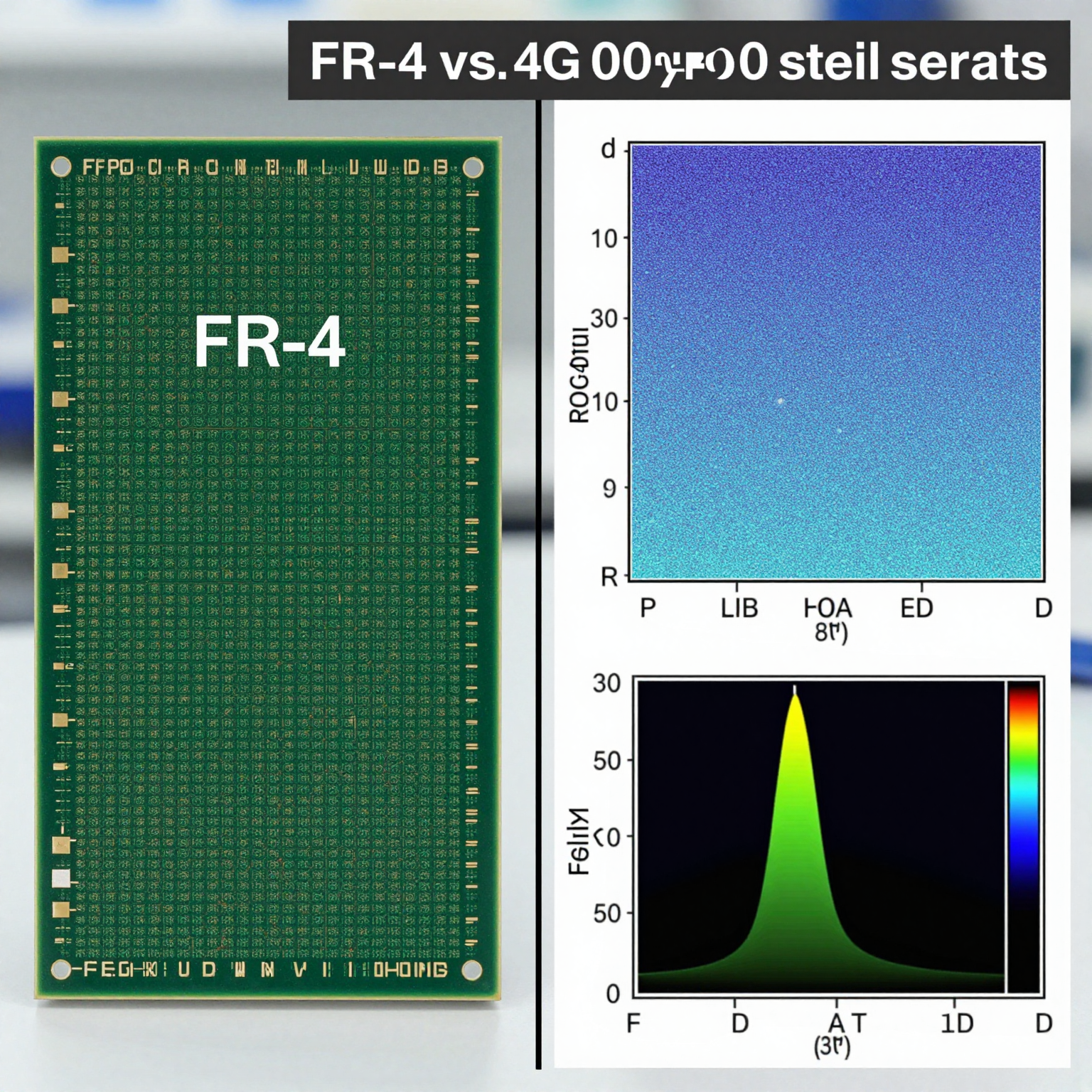
Not all PCB materials are created equal. Standard FR-4 substrates, commonly used in digital boards, exhibit high dielectric loss and inconsistent Dk (dielectric constant) at RF frequencies. This leads to increased signal loss and phase instability.
Instead, designers should opt for specialized laminates such as:
- Rogers RO4000 series
- Tachyon 100G
- Isola I-Tera
- Panasonic Megtron 6
These materials offer lower loss tangents (Df), stable Dk over frequency, and better thermal performance — crucial for maintaining signal integrity in high frequencies PCB applications.
3. Minimizing Parasitics
Parasitic capacitance and inductance become significant at GHz frequencies. Components like capacitors and resistors may exhibit self-resonant frequencies (SRF) where they stop behaving ideally.
Best practices include:
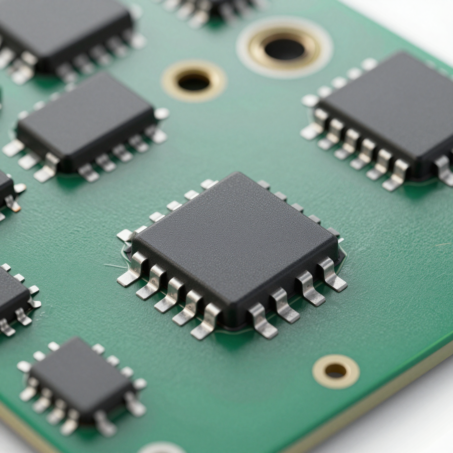
- Using smaller package sizes (e.g., 0402, 0201)
- Placing bypass capacitors close to IC power pins
- Avoiding long stubs and unnecessary vias
- Employing surface-mount technology (SMT) exclusively
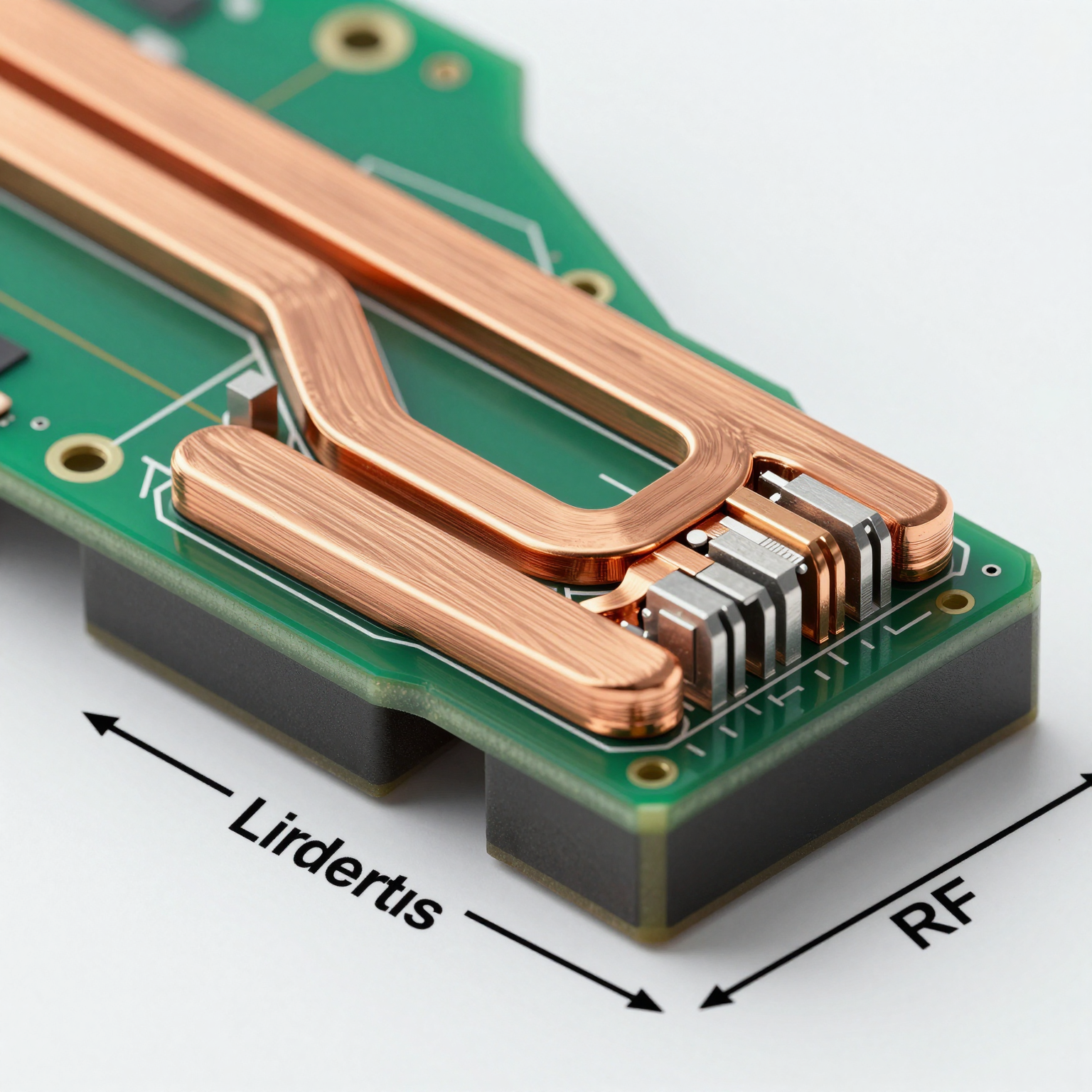
Even the choice of via type matters. Blind and buried vias reduce stub length and improve signal quality compared to through-hole vias.
4. Grounding and Return Paths
A solid ground plane is essential for providing a low-impedance return path for RF signals. Without it, return currents take unpredictable paths, increasing loop area and radiating EMI.
In multilayer RF PCBs, dedicate at least one full layer to ground. Ensure continuous planes without splits or slots under RF traces. Use multiple ground vias near connectors and ICs to minimize inductance in the return path.
Avoid “star grounding” schemes common in analog circuits; instead, use a unified ground plane approach optimized for high-speed return current flow.
Best Practices for RF PCB Layout
Effective layout techniques are key to preserving signal integrity. Here are proven strategies used by experienced RF engineers:
Use Proper Transmission Line Structures
Common transmission line types in RF PCB design include:
- Microstrip
- Stripline
- Coplanar waveguide (with or without ground)
Each has its own advantages depending on isolation needs, loss budget, and manufacturability. Microstrip lines are easy to fabricate and suitable for most surface-layer routing, while striplines offer better shielding within inner layers.
Ensure accurate modeling of these structures using impedance calculators and EM simulation tools.
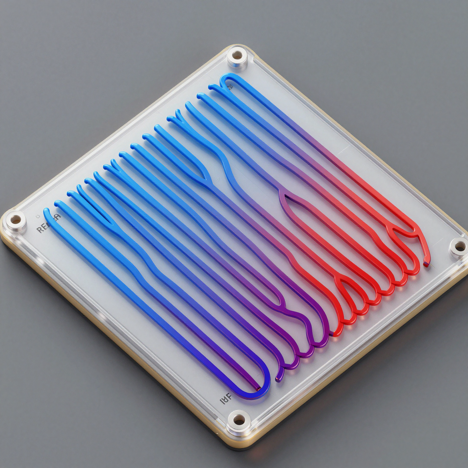
Maintain Symmetry and Minimize Discontinuities
Sharp corners in traces create impedance variations and potential radiation points. Always use curved or mitered bends (45° or rounded) when changing direction.
Similarly, avoid sudden changes in trace width, layer jumps without proper stitching, or placing components directly in high-speed paths.
Isolate Sensitive Traces
Keep RF traces away from digital or noisy power lines. Use physical separation, guard traces (grounded), or even separate board sections when possible.
Shielding cans can be added post-assembly to contain emissions and protect sensitive nodes.
Optimize Power Delivery Network (PDN)
The PDN must provide stable voltage with minimal noise across the entire frequency spectrum. Use multiple decoupling capacitors with different values to cover various frequency bands.
Place bulk capacitors near power inputs and high-frequency ceramics close to active devices. Use low-inductance layouts with short connections.
Prototyping High Frequencies PCB: From Design to Validation
Creating a functional High Frequencies PCB Prototype is a critical step in validating your RF design. It allows you to test real-world performance, identify unforeseen issues, and refine the layout before mass production.
However, prototyping RF boards requires more than just quick-turn fabrication. You need:
- Accurate material replication
- Tight impedance control
- Precision etching and lamination
- Rigorous testing protocols
Many prototype services cut corners on material specs or tolerance control, which defeats the purpose of testing signal integrity.
At SUNTOP Electronics, we support true-to-spec RF PCB prototypes using the same processes and materials intended for final production. Our team works closely with clients to review stack-ups, verify impedance calculations, and recommend optimizations early in the process.
We also offer comprehensive PCB quality testing including TDR (Time Domain Reflectometry), network analysis, and visual inspection to validate signal performance.
How SUNTOP Electronics Supports RF PCB Development
As a full-service PCB assembly manufacturer, SUNTOP Electronics provides end-to-end solutions tailored to the demands of modern RF applications.
Our capabilities include:
- Advanced PCB fabrication with impedance-controlled multilayer stacks
- Support for hybrid designs (FR-4 + Rogers)
- Precision SMT assembly with X-ray inspection
- Component sourcing for hard-to-find RF parts
- Full turnkey and consignment options
Whether you're developing a millimeter-wave sensor, a 5G front-end module, or a satellite transceiver, our engineering team collaborates with yours to ensure manufacturability, reliability, and performance.
We follow a rigorous 6-step quality control process to catch defects early and deliver consistent results — especially vital in mission-critical RF systems.
From High Frequencies PCB Prototype to volume production, we’re equipped to handle complex RF assemblies with confidence.
Final Thoughts: Partnering for Success in RF Design
Designing for high frequencies isn't just about following rules — it's about understanding the physics of electromagnetic waves and applying practical engineering judgment.
While simulation tools are powerful, nothing replaces building and testing a real prototype. But to get meaningful results, your prototype must reflect actual production conditions — right down to materials, tolerances, and assembly methods.
If you're working on an RF project and need expert support in RF PCB design, prototyping, or assembly, don’t go it alone. Partner with a manufacturer who understands both the science and the craft of high-frequency electronics.
Ready to bring your RF innovation to life? Get a PCB quote today and let SUNTOP Electronics help you achieve signal integrity excellence.