PCB Board: The Backbone of Modern Electronics
Heros Rising
What is a PCB Board?
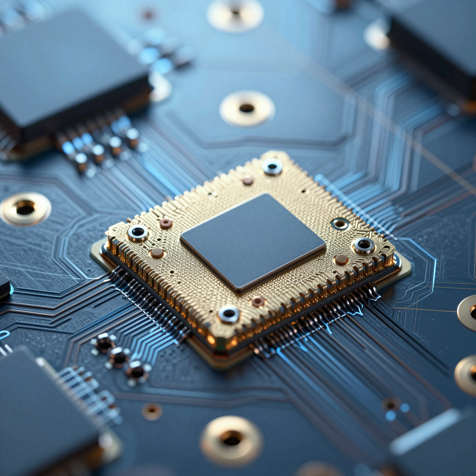
At the heart of nearly every electronic device lies a crucial component known as the PCB board, or Printed Circuit Board. This thin board made from materials like fiberglass, composite epoxy, or other laminates serves as the foundation for mounting and connecting electronic components such as resistors, capacitors, and integrated circuits. The PCB board replaces the older method of point-to-point wiring with a more reliable, compact, and mass-producible solution.
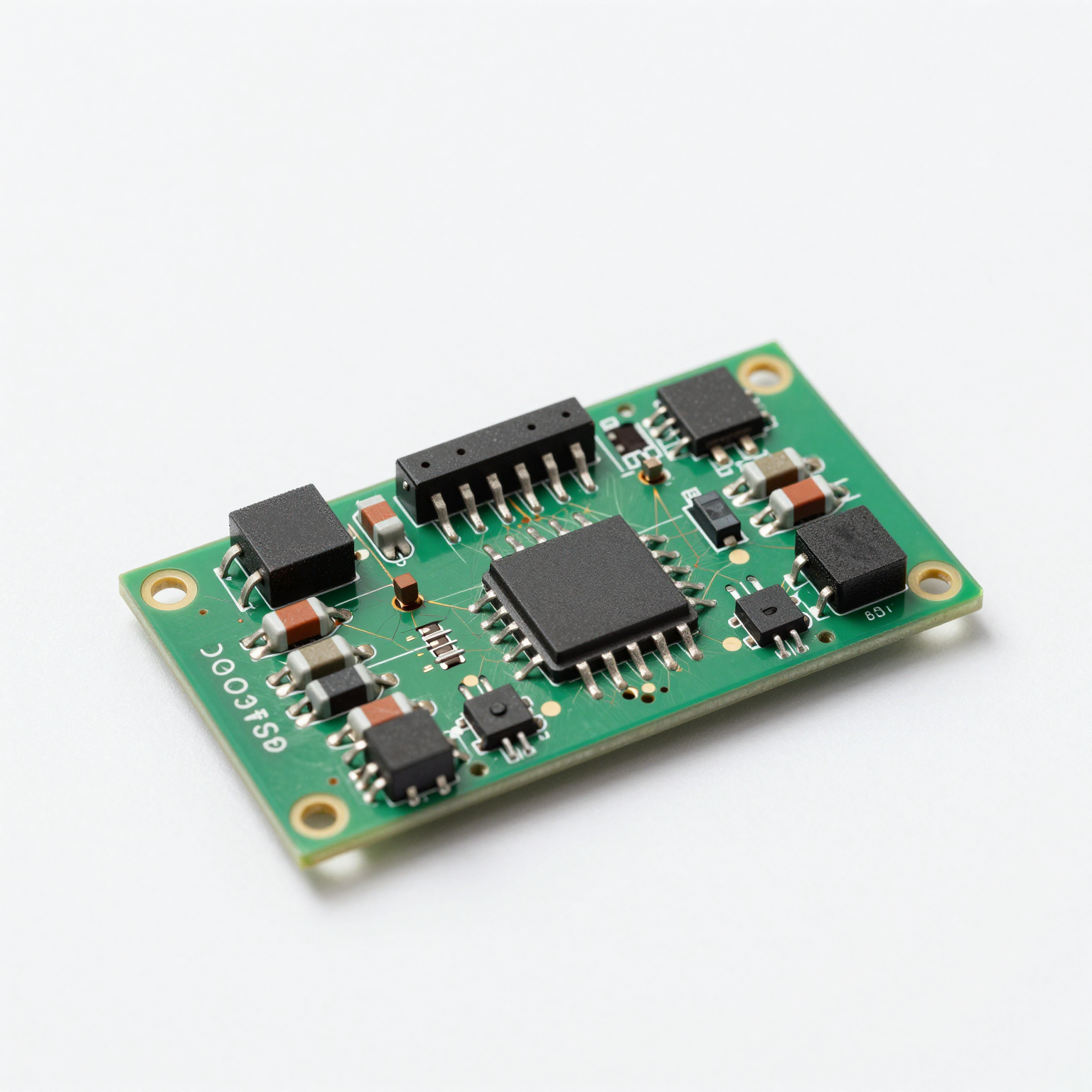
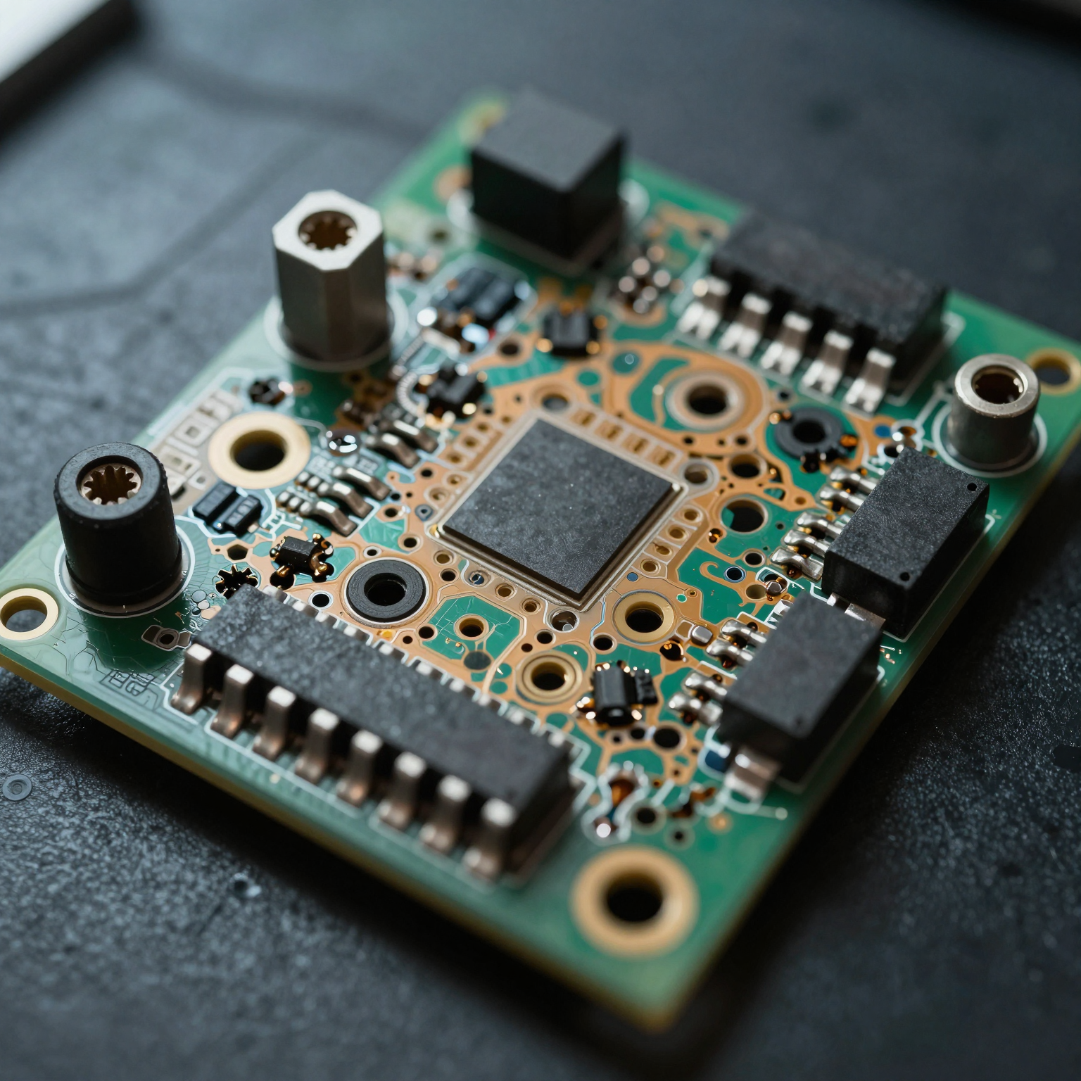
A typical PCB board consists of multiple layers of copper traces embedded between insulating materials. These copper pathways—also called conductive tracks—allow electrical signals and power to flow between components. By precisely routing these connections, engineers can design complex circuits that are both efficient and durable.
The use of a PCB board enables automation in electronics manufacturing, reduces wiring errors, improves repairability, and allows for miniaturization. From smartphones and laptops to medical devices and automotive systems, the PCB board plays an indispensable role in modern technology.
How Does a PCB Board Work?
The functionality of a PCB board hinges on its ability to provide mechanical support and electrical connectivity using etched copper lines. When components are soldered onto the surface of the PCB board, they become part of an interconnected network governed by the layout of the conductive paths beneath.
Each trace on the PCB board is designed to carry specific signals or voltages. For example, one path might deliver 3.3V power to a microcontroller, while another transmits high-speed data between memory chips. Designers use specialized software—commonly referred to as Electronic Design Automation (EDA) tools—to create schematics and convert them into physical layouts suitable for fabrication.
Once manufactured, the PCB board undergoes rigorous testing to ensure signal integrity, impedance control, and absence of short circuits or open nodes. Advanced boards may include features like blind/buried vias, impedance matching, and thermal management layers—all engineered during the PCB board design phase.
Types of PCB Boards
Not all PCB boards are created equal. Depending on the application requirements, different types of PCB boards are used:
Single-Sided PCB Boards
This is the simplest form of a PCB board, where components and copper traces are located on only one side of the substrate. Commonly found in low-density designs such as calculators, LED lighting, and basic power supplies, single-sided PCB boards are cost-effective and easy to manufacture.
Double-Sided PCB Boards
Double-sided PCB boards feature conductive layers on both the top and bottom surfaces. Components can be mounted on either side, and electrical connections between layers are made through plated-through holes (vias). These PCB boards are widely used in telecommunications equipment, instrumentation, and control systems due to their increased circuit density.
Multilayer PCB Boards
For complex applications requiring high-speed processing or extensive interconnections, multilayer PCB boards are employed. These consist of three or more layers of conductive material separated by insulating dielectrics and bonded together under heat and pressure. Examples include server motherboards, radar systems, and advanced medical imaging devices. Multilayer PCB boards allow for greater functionality in smaller footprints.
Flexible and Rigid-Flex PCB Boards
Flexible PCB boards (Flex PCBs) are made from flexible plastic substrates like polyimide, allowing them to bend and conform to tight spaces. They're ideal for wearable tech, foldable displays, and aerospace systems. Rigid-flex PCB boards combine rigid and flexible layers into a single unit, offering structural stability with dynamic flexibility.
High-Density Interconnect (HDI) PCB Boards
HDI PCB boards incorporate finer lines and spaces, smaller vias, and higher connection pad density than conventional PCB boards. Used in smartphones, tablets, and HD cameras, HDI technology supports faster signal transmission and improved reliability in compact packages.
The PCB Board Manufacturing Process
Creating a functional PCB board involves several precise steps, each critical to ensuring performance and longevity.
Step 1: Design and Layout
Engineers begin by designing the circuit schematic and converting it into a physical layout using CAD tools. This includes placing components, defining trace widths, setting layer stackups, and ensuring compliance with design rules.
Step 2: Printing the Design
The finalized layout is printed onto a special film called a "photomask" used in later etching stages. This step ensures accurate reproduction of the intended circuit pattern.
Step 3: Substrate Preparation and Copper Lamination
A base material—typically FR-4 fiberglass—is coated with a layer of copper on one or both sides. In multilayer PCB boards, multiple pre-etched cores are aligned and laminated together under high temperature and pressure.
Step 4: Etching
Using chemical processes, unwanted copper is removed, leaving behind only the desired conductive traces. This defines the actual circuit pathways on the PCB board.
Step 5: Drilling and Plating Vias
Precision drilling creates holes for through-hole components and vias. These holes are then electroplated to establish electrical connections between layers in double-sided and multilayer PCB boards.
Step 6: Solder Mask Application
A protective solder mask is applied over the copper traces to prevent oxidation and accidental shorts. Openings in the mask expose pads where components will be soldered.
Step 7: Silkscreen and Surface Finish
Component labels, logos, and reference indicators are printed via silkscreening. A final surface finish—such as HASL (Hot Air Solder Leveling), ENIG (Electroless Nickel Immersion Gold), or OSP (Organic Solderability Preservative)—is applied to protect exposed copper and enhance solderability.
Step 8: Testing and Quality Assurance
Finished PCB boards undergo various tests including continuity checks, AOI (Automated Optical Inspection), X-ray inspection, and flying probe testing to verify integrity before assembly.
You can learn more about this process in our detailed guide on the PCB manufacturing process.
Applications of PCB Boards Across Industries
The versatility of the PCB board makes it essential across numerous sectors:
- Consumer Electronics: Smartphones, TVs, gaming consoles, and home appliances rely heavily on compact, high-performance PCB boards.
- Medical Devices: From pacemakers to MRI machines, PCB boards must meet strict safety and reliability standards.
- Automotive Systems: Modern vehicles use dozens of PCB boards in engine control units, infotainment systems, ADAS, and electric vehicle battery management.
- Industrial Equipment: Robotics, PLCs, sensors, and motor drives depend on ruggedized PCB boards capable of operating in harsh environments.
- Telecommunications: Routers, switches, base stations, and fiber-optic gear utilize high-frequency PCB boards optimized for signal integrity.
- Aerospace and Defense: Mission-critical avionics and guidance systems employ advanced PCB boards built for extreme durability and performance.
Advantages of Using PCB Boards
Using a PCB board offers numerous benefits over traditional wiring methods:
- Compactness: Enables miniaturization of electronic devices.
- Reliability: Reduces loose wires and faulty connections.
- Scalability: Supports automated assembly for mass production.
- Repairability: Clearly labeled components and standardized layouts simplify troubleshooting.
- Cost-Efficiency: Lowers long-term production costs despite higher initial tooling expenses.
- Improved Electrical Performance: Controlled impedance and reduced electromagnetic interference (EMI) in well-designed PCB boards.
Choosing the Right PCB Board for Your Project
Selecting the appropriate type of PCB board depends on several factors:
- Complexity of Circuitry: Simple circuits may only need single-sided boards; complex digital systems require multilayer or HDI PCB boards.
- Size Constraints: Miniature devices benefit from HDI or flexible PCB boards.
- Environmental Conditions: Harsh environments call for robust materials and protective coatings.
- Production Volume: High-volume runs favor automated-compatible PCB boards with standardized footprints.
- Budget: While advanced PCB boards offer better performance, they come at a higher cost.
Working with an experienced PCB assembly manufacturer ensures your design translates into a reliable, manufacturable product.
Future Trends in PCB Board Technology
As technology evolves, so too does the PCB board. Emerging trends include:
- Miniaturization: Continued push toward smaller components and tighter pitches.
- Higher Speeds: Development of ultra-low-loss materials for 5G, AI accelerators, and quantum computing hardware.
- Embedded Components: Integration of passive and active elements within the PCB board itself to save space.
- Sustainable Materials: Research into biodegradable substrates and lead-free manufacturing techniques.
- Smart PCBs: Incorporation of sensors and self-diagnostic capabilities directly into the PCB board structure.
These innovations promise to expand the capabilities of PCB boards far beyond current limits.
Conclusion
The PCB board remains a cornerstone of modern electronics, enabling the sophisticated devices we rely on daily. Whether you're developing a prototype or scaling up production, understanding the fundamentals of PCB board design, types, and manufacturing is essential. As demands for speed, size, and efficiency grow, the evolution of PCB board technology will continue to drive innovation across industries.
For those seeking expert support in bringing their ideas to life, partnering with a trusted provider ensures quality, reliability, and timely delivery.